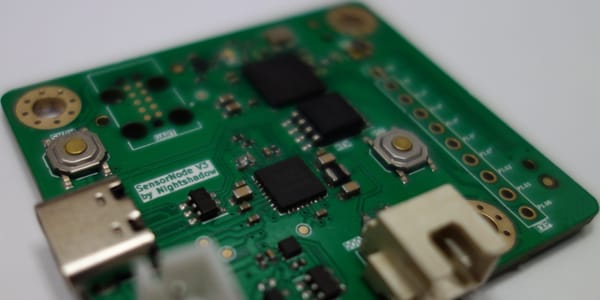
Blog - Sensor Node V4.00
Introduction
This is the next version of the Sensor Node. Details on the previous version can be found in the older blog post on the [Sensor Node V3.00](https://blog.preisch.cloud/sensor-node-v3-0/)
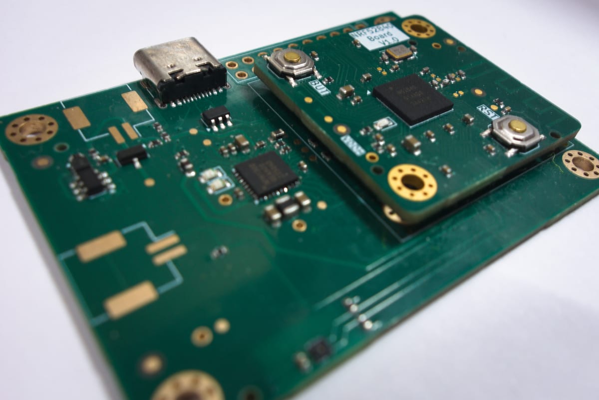
For this version I decided to change the topology and move to a two PCB solution:
- NRF52840 MCU Board V1.00
- NRF52840 Base Board V1.00
To connect the board a mezzanine connector similar to the raspberry pi compute module will be used. This approach allows to reuse the MCU Board for other projects as well. So lets first dive into both boards separately and look at the overall system afterwards.
NRF52840 SOC V1.00
repository https://github.com/Nightshadow1258/NRF52840_SOC
Micro Controller Unit (MCU) Board
main components / Integrated Circuits (ICs):
- MCU: NRF52840
- PCB antenna
- Reset Button
- User LED
NRF52840 Base Board V1.00
main components / ICs:
- PMIC: NPM1300
- Temperatue/Humidity Sensor: SHT4x
- Battery protection: BQ29700
Sensor Node V4.00
Firmware with Zephyr
For developing the firmware I will be relying on the open source real-time operating system (RTOS) called Zephyr Project. Here is a link to my repository for this hardware version NRF_Sens_Module. Since the manufacturer of the NRF52840 nordic semiconductor is heavily contributing to the Zephyr Project the support for the MCU NRF52840 and the PMIC NPM1300 is great.
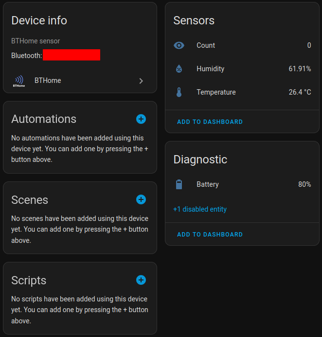
BTHome Setup
see below the added Sensor in the homeassistant dashboard
Measurements
Load Crystal
For this test I tried to measure the Crystal Oscillator frequency with my Oscilloscope and compare the result.
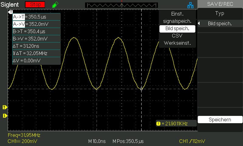
added \(12\,pf\) in parallel to have a total load capacitance of \(24\,pf\).
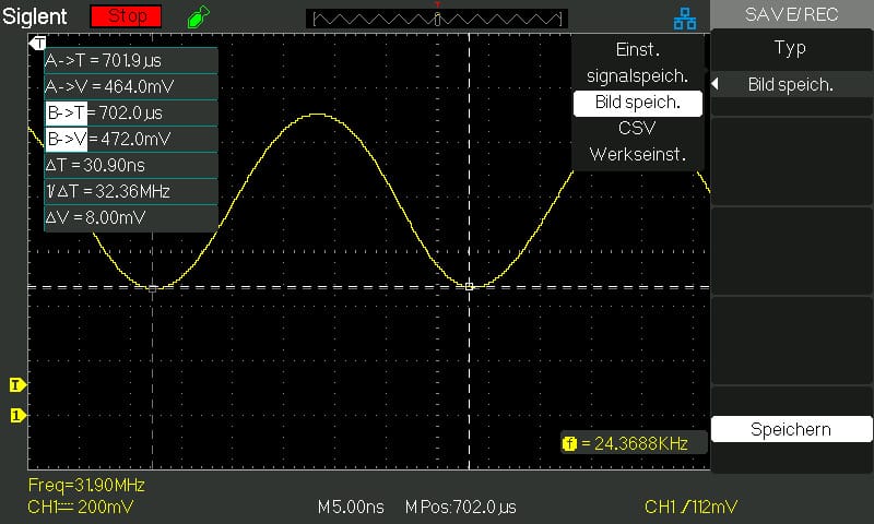
Oscilloscope Measurement Setup
Summary
No chance to see the difference with my oscilloscope (Siglent SDS 1102CML+). Probably because of the limited bandwidth of 100MHz and also the additional loading due to the capacitance of the probes them self. Ideally I would like to use a universal frequency counter to compare the to different configurations, bit I do not have one at hand :(
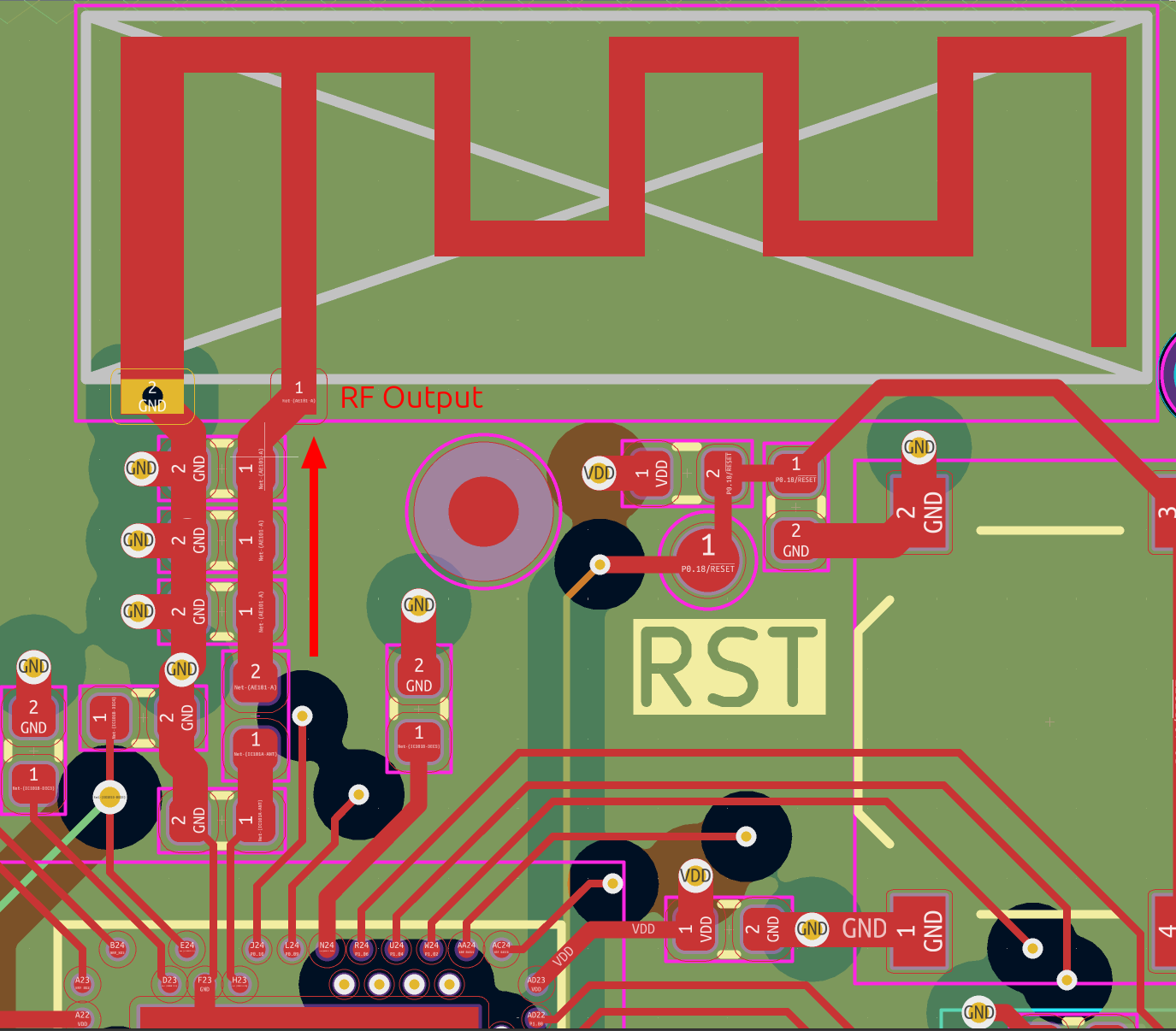
Antenna
list of issues:
- Inductor was not rated for \(2.4\,GHz\) operation -> new one has resonance frequency at \(5.5\,GHz\) show image of curve
- Impedance matching not done at all. Next revision I will use coplanar traces with the GND Plane on the bottom layer. The inner layer will have a keep-out zone. This will reduces stray capacitance compared to using an inner layer as the reference plane for the coplanar trace.
- add matching circuit for antenna in addition to impedance matching circuit.
Layout design antenna
Inductance Specs
The initial inductor used is the SDCL1005C4N7STDFM02. In my initial design I did not think about the inductor at all. In hindsight this was a mistake, since it has a frequency response curve like every other components.
See the characteristics from the datasheet below:

From the Inductance vs Frequency (left upper plot) it becomes apparent that in the BLE range of \(2.4\,GHz\) this inductor will have a different compared to the nominal value of \(4.7\,nH\). It should still be in an acceptable range though (the x-axis goes up to \(3\,GHz\)). The Q-Factor peaks around the \(2.4\,GHz\) for the \(5.6\,nH\) type and should be similar for the \(4.7\,nH\) version I am using.
Therefore I would say that the inductor is acceptable for this use case. Nonetheless, I will replace it with a better type in the next version to be on the safe side.
Measurement Spectrum Analyzer
These measurements are needed to draw quantifiable conclusions and check if the improvements had an impact. Since changes to the layout (track width, spacing, antenna design) require to manufacture a new hardware revision, the first measurements are for the improvements than can be tested with the initial hardware revision. This includes the following points:
- change of inductor (part used: MLG1005S4N7STD25)
- optimization of load capacitance of the high frequency crystal Oscillator (HFXO)
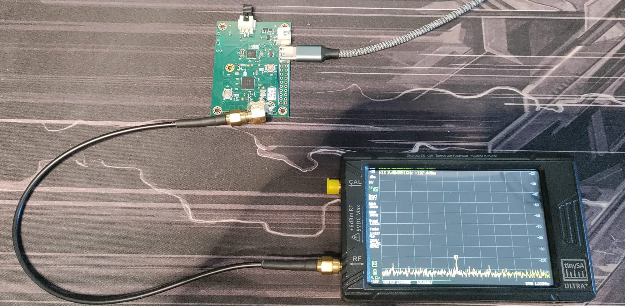
For the measurement atinySA ULTRA+was used.
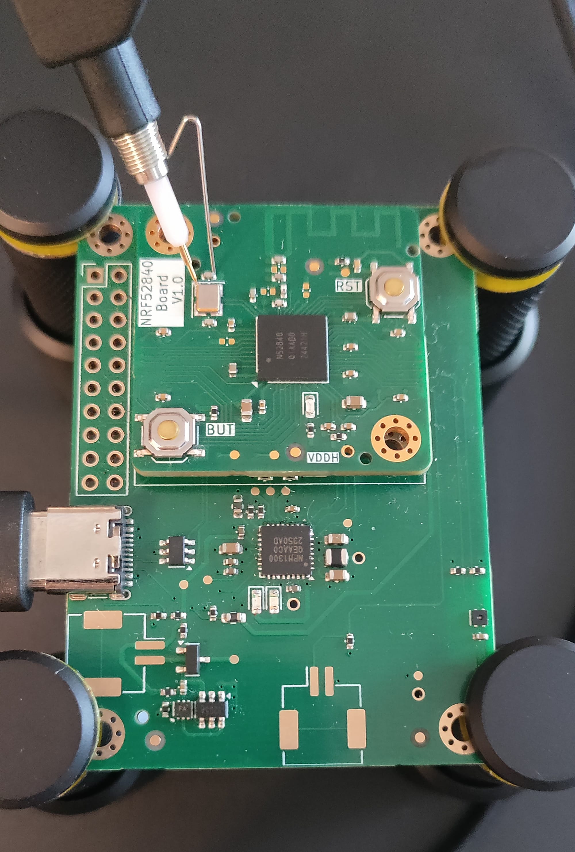
Due to suboptimal soldering the SMA connector to measure the MCU RF output is only
Measurement Setup
See below the modification that were done to the PCB for this measurement
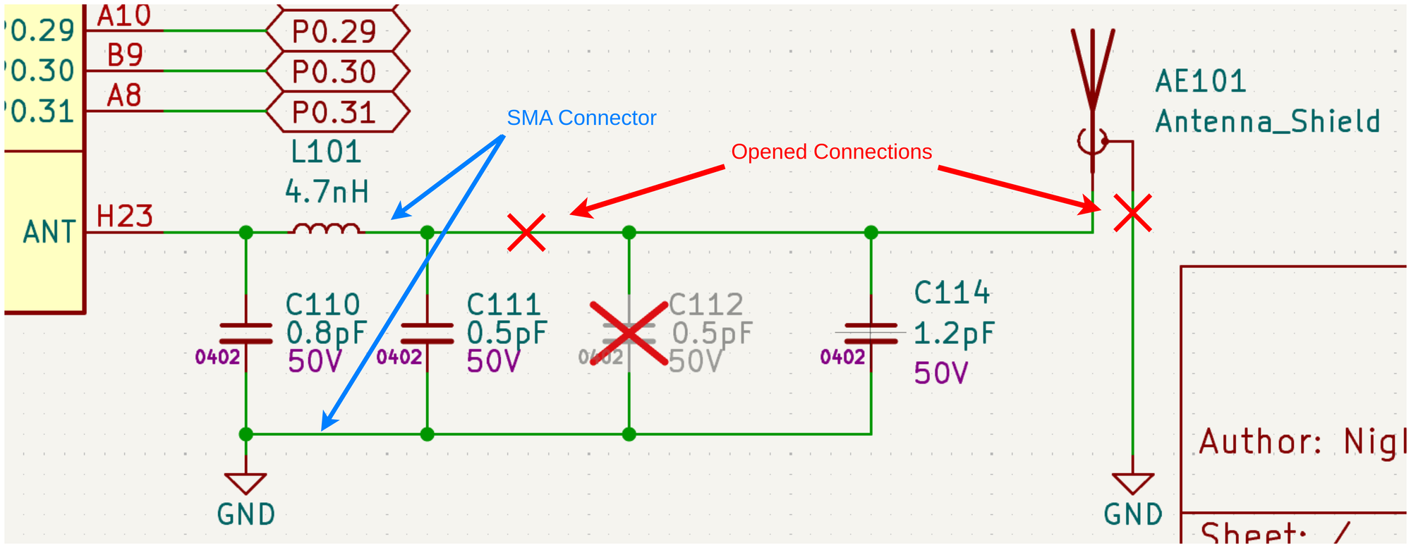
The Antenna GND was removed by cutting the connection on the PCB. Also the Antenna itself was disconnected by cutting the PCB trace to it. From this point the SMA connector was feed and connected to GND. The SMA connector was than connected to the tinySA ULTRA+ as shown below:
tinySA ULTRA+Measurement with CL=12pf and SDCL1005C4N7STDFM02
First a baseline measurement the default hardware configuration was tested to have a baseline to compare against later. The measurement was stored as a .csv file and plotted below:
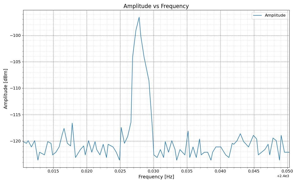
The measured peak is at a frequency of \(2.4,GHz\) + \(278,kHz\) with an amplitude of \(-96.594,dBm\)
Measurement with 24pf and MLG1005S4N7STD25
The same measurement was done after changing the loading capacitors from \(12,pf\) to \(24,pf\) and the inductor to the type MLG1005S4N7STD25.
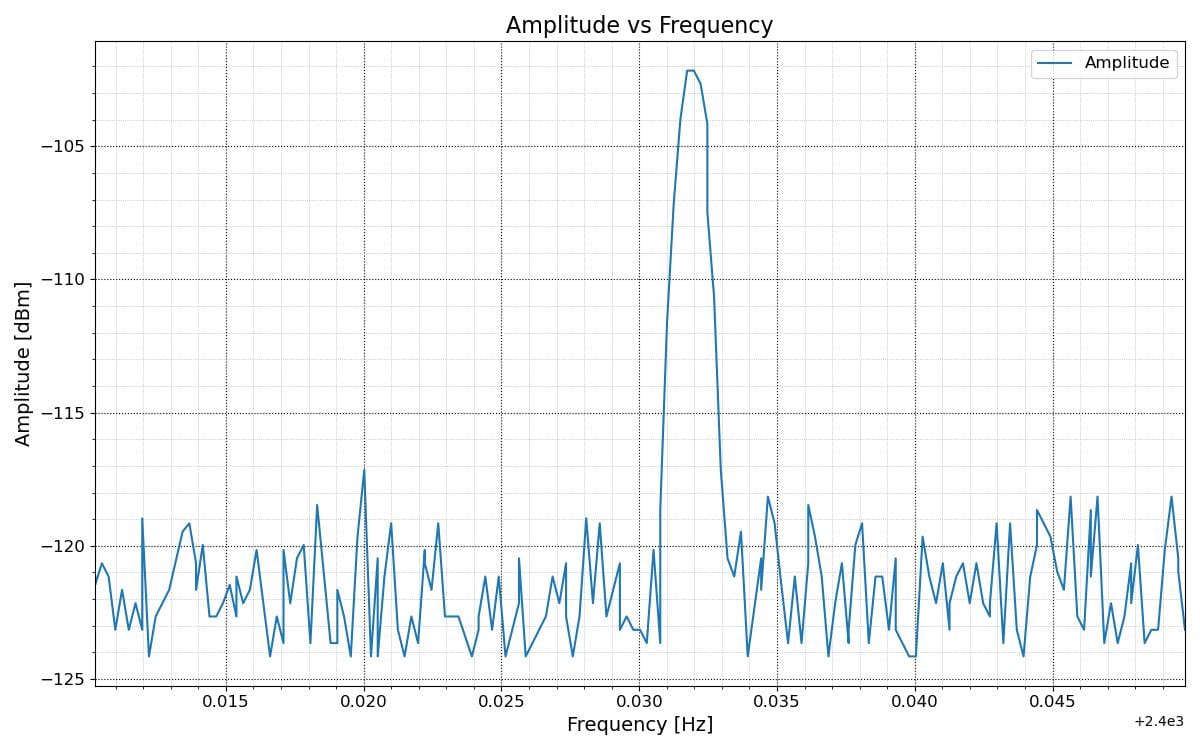
This time the measured peak is at a frequency of \(2.4,GHz\) + \(319,kHz\) with an amplitude of \(-102.156,dBm\)
Changing the load capacitor shifts the output frequency slightly up. But I do not trust this measurement completely, since this is the first time I am using this measurement equipment.
From my research online if the load capacitance increases the frequency should decrease. This also makes sense on a physical level, since a higher capacitance will slow down the rise time of signals (higher charge time) and therefore decreasing the frequency.
Improvements for next time
For each of the measurements a re-calibrate of the tinySA ULTRA+ should be done. In addition only one change should be done at a time. Here I changed the load capacitance and the inductor at the same time
Antenna Design upgrades
The antenna design is based on the NRF52840 USB Dongle. Since the PCB stackup will differ from the reference design, I would like to verify the correct design in Simulation. This will be a good learning opportunity, since I never did any antenna simulations before. I should have some familiarity due to my electronic and telecommunication bachelors degree and should be able to achieve some satisfactory results.
Simulation
In the future I would also like to verify my design with a simulation and to visualize the resulting electro-magnetic field. This will be a lot of work and requires its own post in the future and depends when I get the time to dive into it.
Issues and Improvements for next revision
NRF52840 SOC V2.00 changes
- BaseBoard add Antenna keepout zone for Modul mounting footprint
- change the Inductor to high frequency one.
- update Crystal Oscillator and loading capacitors
- add low frequency oscillator for low power mode
- update antenna design and layout (add matching network for antenna as well)
- remove the LED and current limit resistor -> not needed and will only consume power and place also reduces cost slightly as well 😄
NRF52840 Base Board V1.00
- change the Mezzanine connector to one with retention clips for better stability
- postponed due to minor issue -> reuse with SOC V2.00
I will make a new blog post when I get the V2.00 of the SOC board. There I will also make some comparisons to the V1.00 in terms of the antenna design (layout and schematic) and measurements. Until then happy debugging!