Sensor Node V3.0
Introduction
This is the third version of my small IoT project I call Sensor Node. The general idea is to create a power efficient IoT device that can monitor different parameters like:
- Temperature
- Humidity
- Door/Window State
- Lighting
- Movement
- etc...
The goal is to place them in each room and connect them to Home Assistant for logging and viewing the data. First lets review what V2.0 was capable of and what could be improved.
Recap of V2.00
The previous versions used a ESP32 as the brain and connected over Wifi with a MQTT server.
MQTT is a subscriber and publisher based communication protocol, that is well supported by Home Assistant and the Arduino development framework.
The main sensor of the system is a SHT40 temperature and humidity sensor, that connects via I2C to the MCU (ESP32). The whole system is powered by a 18650 lithium-ion cell.
Issues with V2.00
The power draw of the EPS32 variant was to too high even when waking up every 15 minutes to grab the sensor data and publishing it, the battery ran out after only one or two moths. The main reason is that the communication over Wifi takes a lot of juice. Therefore I decided to use the NRF52840 as the new MCU and relying on Bluetooth Low Power to transmit the data. For that I want to use the BTHome (https://bthome.io/) protocol, which is supported by Home Assistant. In addition I am moving away from the Arduino Framework to the Zephyr project (https://www.zephyrproject.org/).
Sensor Node V3.00
The design file can be found on my github repo https://github.com/Nightshadow1258/Sensor_Node/tree/V3.00. The other Versions are stored as different branches there as well.
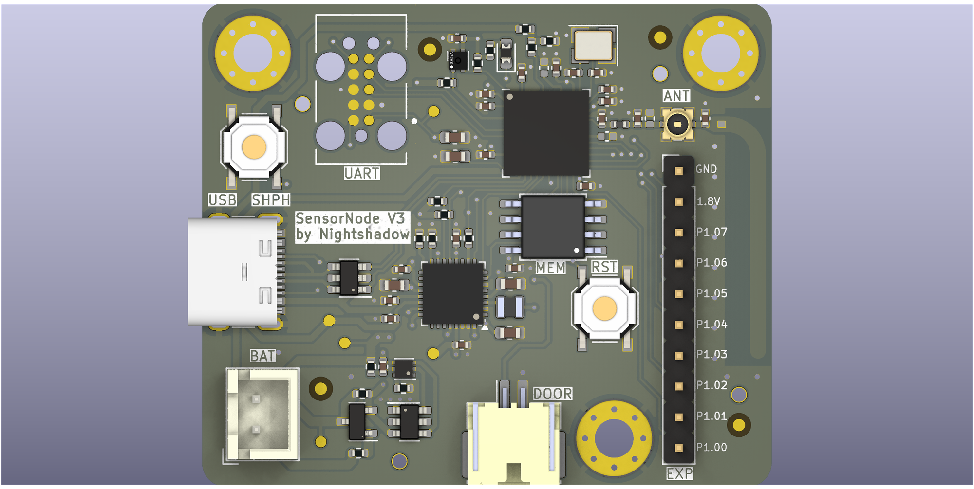
Hardware Design
The pdf export of the schematic can be found here: https://github.com/Nightshadow1258/Sensor_Node/blob/V3.00/Documents/SCH_Sensor_Node_V3.00.pdf.
The schematic differs a bit from the original design, since I updated most of the issues listed below already and I do not have the full history anymore.
The design uses the NPM 1300 as a Power Management IC (PMIC) to generate the required voltage rails to power the NRF52840 MCU. In addition the PMIC also includes charging for single lithium-ion cells, when power via USB. For added safety a separate battery protection IC (BQ29700) is used to provide the following protections:
- overcurrent protection
- overcharge protection
- overvoltage protection
- undervoltage protection
The PMIC is either supplied by the 5V VBUS of the USB connector or by a battery.The default buck output voltages can be set via the resistor on the VSET1 and VSET2 pins. VSET1 is fitted with a 47kΩ for a voltage of 1.8V, while second buck output is disabled by pulling VSET2 to GND (0Ω).
The MCU is than supplied by the 1.8V output voltage of the PMIC. The 5V VBUS line is used to power the USB section of the NRF52840, which enables to also use the USB C ports data lines for communication (manly used for debugging during development). A 32MHz external crystal with 12pf load capacitors generate the clock for the MCU. The main programming interface is a Serial Wire Debug (SWD) and a dedicated Universal Asynchronous Receiver / Transmitter (UART) which use a TC2050 connector. This connector requires no header to be fitted and directly connects to the exposed pads, reducing cost and the requires space on the board.
The following peripherals are available and connected to the MCU:
- SHT40 (Temperature and Humidity Sensor) connected via I2C
- MX25R6435F (Flash Storage) connected via QSPI
- NPM1300 (PMIC) connected via I2C
- Reset button to manually reset the MCU
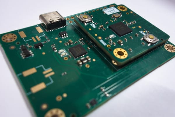
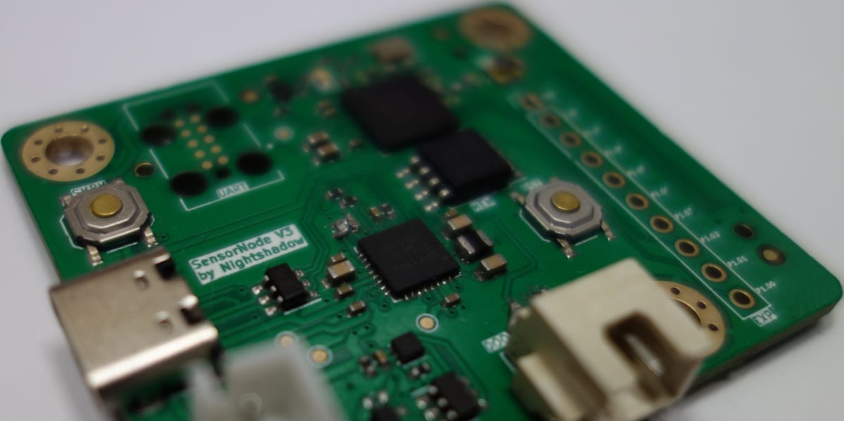
See below a render of the PCB layout and the manufactured Board.
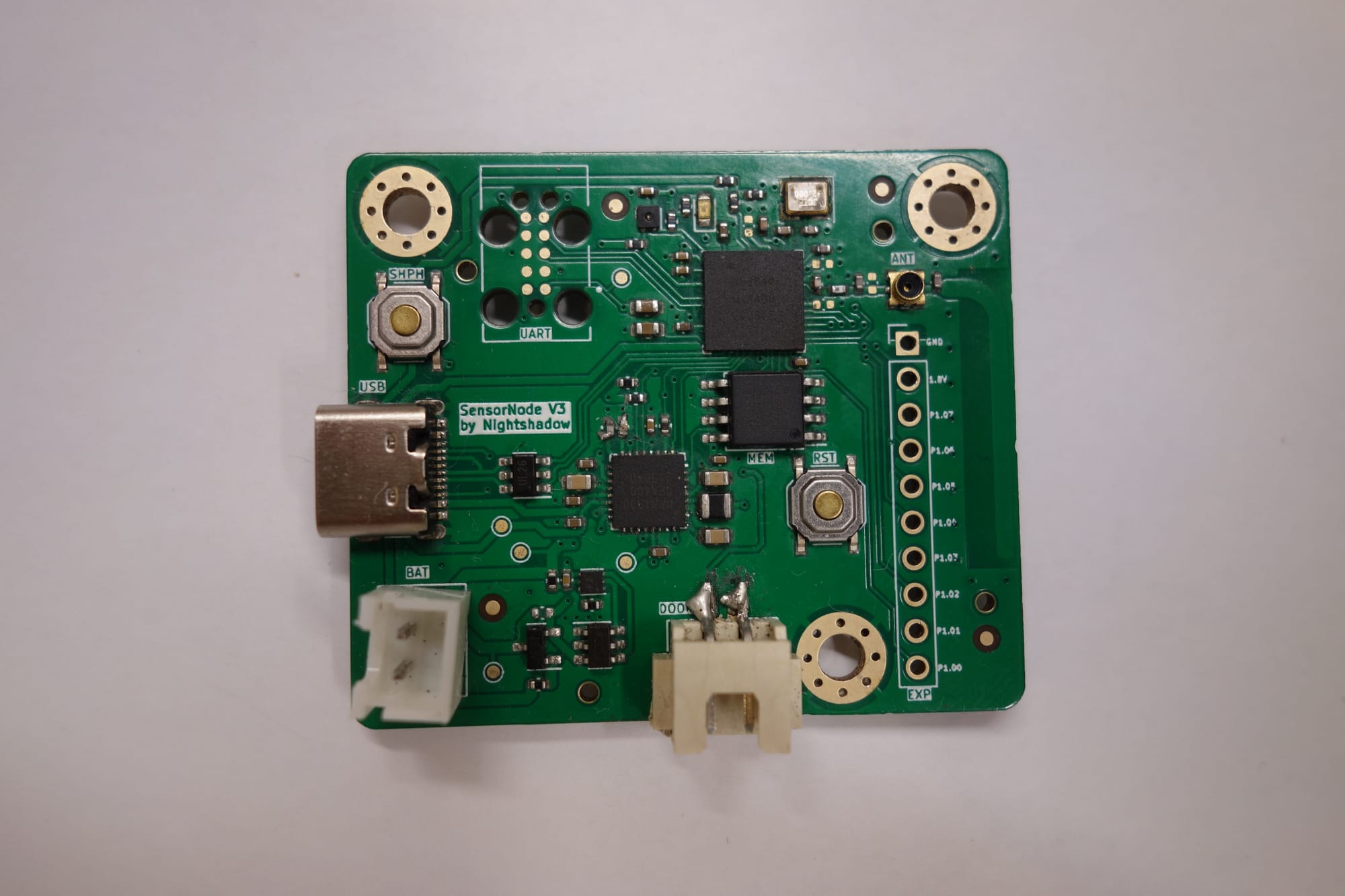
I know not the cleanest soldering job on the connector and the crystal also has seen some better days.
Issues
PMIC
The pins for the VSET1 and VSET2 were swapped, which resulted in the VOUT1 to be disabled and the board not powering up at all. After solving this by swapping the resistors manually the board power up.
MCU flashing
The next big issues was that most of the board could not be programmed, since the debugger could not connected to the MCU. After some experimentation and trying to resolder the MCU IC and applying pressure, I realized that the soldering seems to be the issue. Sadly I was not able to fix most of the boards, but for the next revision I will have to tune the footprint to achieve a higher reliability.
Antenna
The last major problem I ran into was a low transmit and receive range for the Bluetooth. In hindsight this could also have been an issue with the at the time current firmware version.
Antenna Layout:
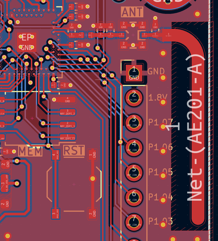
The RF path goes through a matching PI-Filter and through and should be match to an impedance of 50Ω. The antenna has to have a keepout zone for all layers to allow the propagation of the RF signal. To shield the GND plane it is advised to place GND around the antenna.
Conclusion
After all the Issues I had with this revision I decided that it would be best to create a new version that addresses all of the issues above (some foresight I did make new mistakes). All in all for a first design with this MCU and this PMIC I was happy same of the boards work without the need of extensive patching of the hardware design.
The next Version will be tested more thoroughly and I will also share the firmware that I will be using after figuring out the best way to document it.
See you and happy patching!