DIY Motor Controller Board Part II: Timer & ADC Configuration
Intro
This is the second part of my Motor Controller Board Series. You can check out the first Part here. After the hardware design process and the initial testing of the hardware is done, we can dive into the first firmware configuration (done in Zephyr) that we will need for the final version. In this post I will focus on the configuration of the timer output to control the motor as well as the ADC configuration to read the phase currents. I plan to go into more detail of how a BLDC motor works and what we need to spin it in the next part of this series.
Firmware
As mentioned in the introduction, Zephyr is the chosen framework for firmware development. The Firmware can be found on my github page here. This is a good point to evaluate our objectives and determine the ideal path forward. Ideally, this planning happens before designing the hardware, but working with existing hardware often requires creative problem solving ;)!
The primary control objectives for the BLDC motor are:
- Reading all relevant sensor data including phase currents: ($I_A$, $I_B$, $I_C$ ) and the motor position $\varphi_{mech}$
- Calculations to determine the PWM duty cycle for the motor (timer peripheral is used for this)
- applying the PWM duty cycle via the configured timer
Secondary objectives include: - UART shell command interface for testing, debugging and measurements during development
- NTC based Temperature Sensor (not in this post)
- Test Ethernet communication (not in this post)
- Test CAN communication (not in this post)
- use execute-in-place (XIP) with MCUboot to utilize the external flash (not in this post)
store calibration data and board specific data on the external flash (not in this post)
For the control loop we will need a tight timing constraints to achieve adequate control. Therefore the measurement and timer output need to be precisely configured. For the control loop I am targeting $20\,kHz$. In order to achieve this I created the following diagram containing the rough battle plan. I know that the MPS should also be shown here since it is also an input for the controller but I plan to refine and extend this diagram along the way.
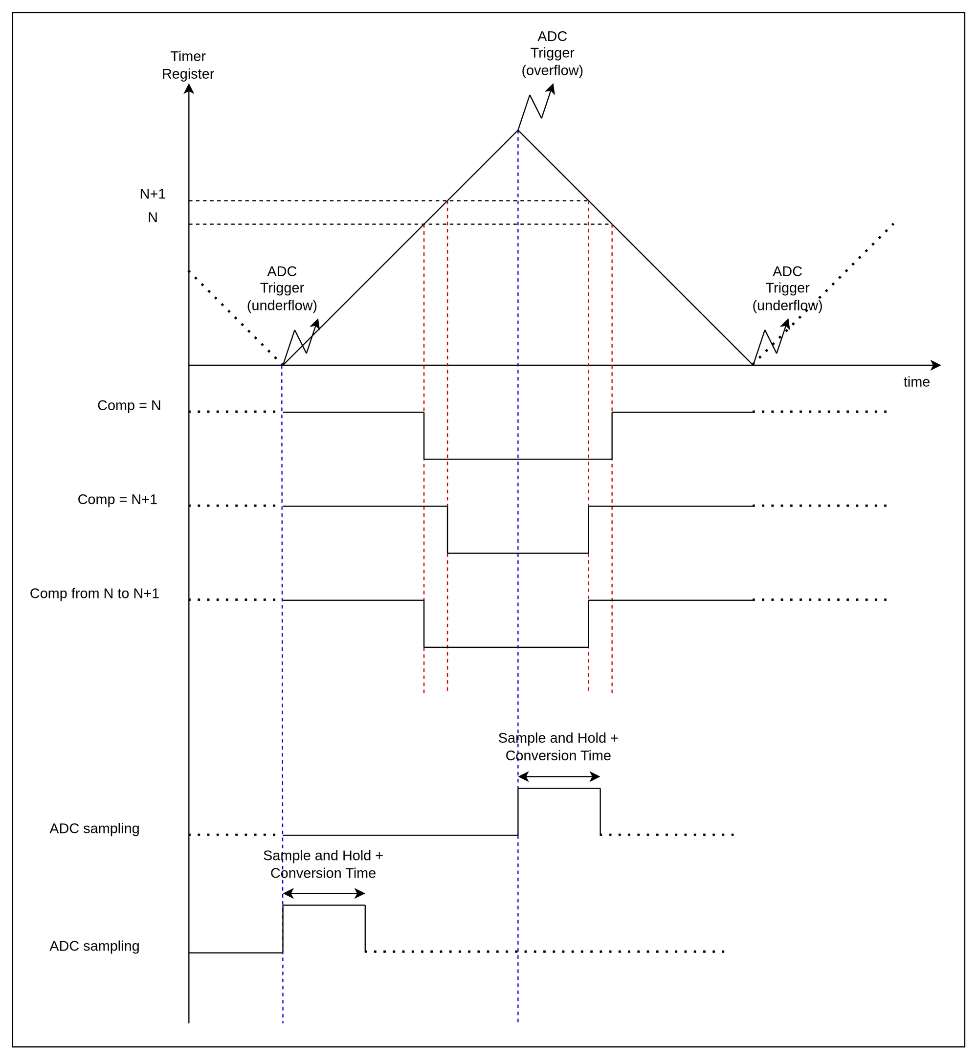
The Timer 1 will be used to generate the PWM signals. This advanced Timer outputs complementary signals and also inserts dead time. Configuring the PWM in center aligned mode with up and down counting modeenables triggering the ADC during the current conducting and non conducting phase, enabling a offset calibration.
Not sure if I will implement this from the get go but in theory that should be possible. An important technical constraint is that current measurement is not possible at $100\,\%$ duty cycle. The exact limit is determined by the total dead time $t_{dead}$ and the settling time of the ADC $t_{ADC,settle}$ . An alternative approach relies on Kirchhoff current law where the sum of all three phase currents equals zero, allowing calculation of the missing phase current from the other two:
$$ I_{A} +I_{B} +I_{C} = 0 \Rightarrow I_{A} +I_{B} = - I_{C}$$
This method is frequently used in electronic speed controllers to reduce cost by eliminating one shunt resistor and one ADC channel. However, safety-critical applications benefit from measuring all three phases to provide a reliable sanity check. So depending on the application either solution can be valid. With this we have a pretty basic architecture to work towards. I decided to start with the Timer configuration and work my way up from there.
Clock Tree Setup
The clock tree relies on an external $16\,MHz$ crystal. I used the STM32CubeMX Software to generate the clock dividers based on that input, followed by configuring the device tree file in Zephyr.
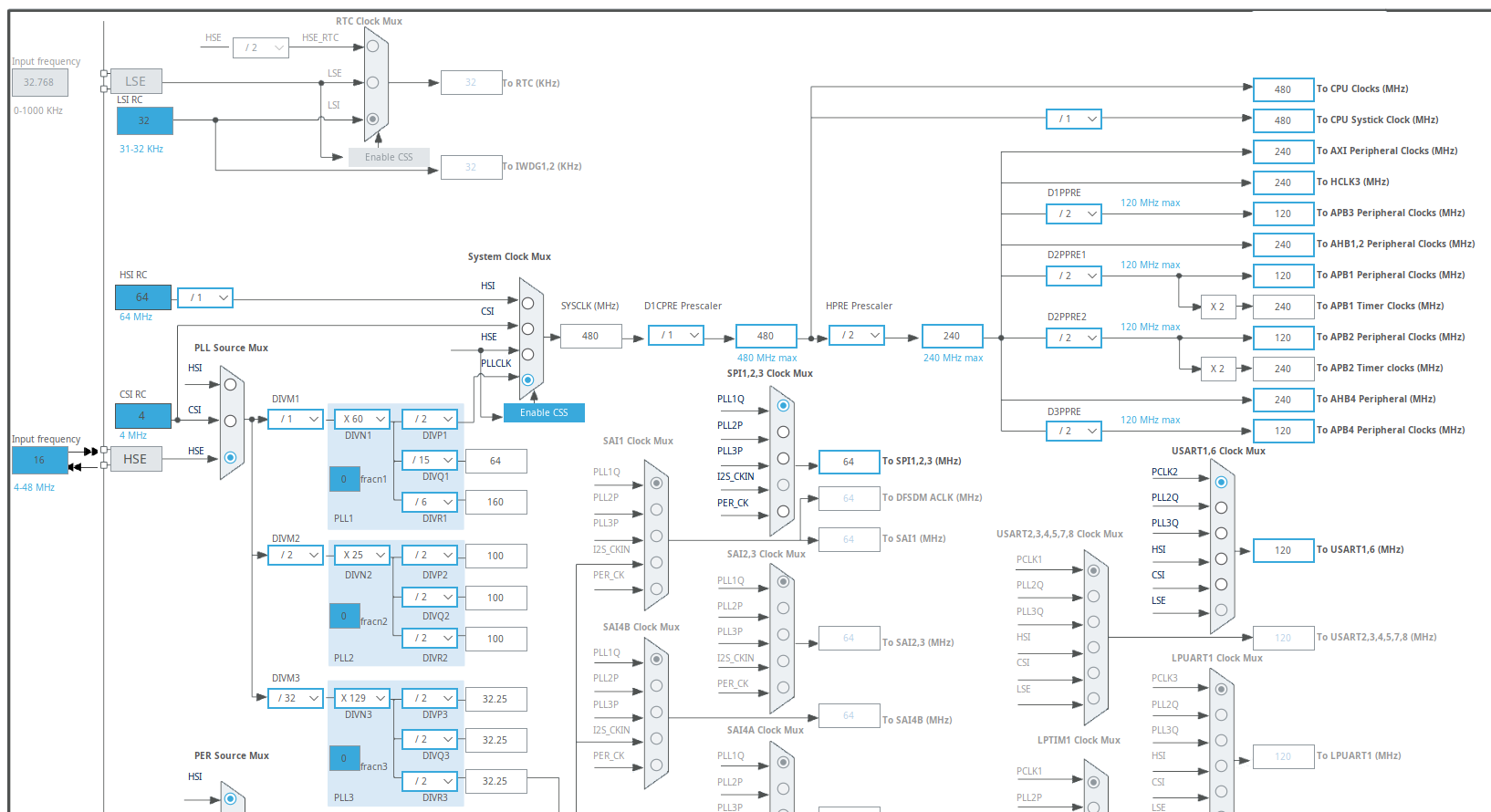
Based on this I configured the clock tree via the device tree file (.dts) in Zephyr as shown below:
&clk_hse {
	clock-frequency = <DT_FREQ_M(16)>;
	status = "okay";
};

&pll {
	div-m = <1>;
	mul-n = <60>;
	div-p = <2>;
	div-q = <15>;
	div-r = <6>;
	clocks = <&clk_hse>;
	status = "okay";
};

&pll2 {
    div-m = <2>;
    mul-n = <25>;
    div-p = <1>;   /* (16 MHz / 2) * 25 / 1 = 100 MHz */
    clocks = <&clk_hse>;
    status = "okay";
};
&rcc {
	clocks = <&pll>;
	clock-frequency = <DT_FREQ_M(480)>;
	d1cpre = <1>;   /* SYSCLK / 1 = 480MHz */
	hpre = <2>;    /* 480MHz / 2 = 240MHz (Max AHB speed) */
	d1ppre = <2>;  /* 240MHz / 2 = 120MHz (APB3) */
	d2ppre1 = <2>; /* 240MHz / 2 = 120MHz (APB1) */
	d2ppre2 = <2>; /* 240MHz / 2 = 120MHz (APB2) */
	d3ppre = <2>;  /* 240MHz / 2 = 120MHz (APB4) */
};
Advanced Timer 1
As already mentioned I will be using the advanced timer 1 of the STM32H750VB to generate center-aligned, complementary PWM Signals for the GDU. In total this will be six PWM Signals two for each of the three phases. In addition I will be using the deadtime insertion capabilities of the timer as well. Strictly speaking I do not strictly need this, since the selected GDU also does dead time insertion, but for the first setup I wanted to be on the safer side. Lets hope that this will not bite me in the ass in the future.
For the configuration the application note AN4013 was quite handy to have around. Since I was unable to use the built-in zephyr API to configure the timer 1 the way I wanted, I had to fall back to configuring it via the HAL Interface. This allows to configure the hardware registers of the MCU directly. The pin mapping still was done in zephyr via the .dts file as shown below:
/* Pin Control Definition */
&pinctrl {
    tim1_ch1n_pe8: tim1_ch1n_pe8 {
        pinmux = <STM32_PINMUX('E', 8, AF1)>;
        drive-push-pull;
    };
    tim1_ch1_pe9: tim1_ch1_pe9 {
        pinmux = <STM32_PINMUX('E', 9, AF1)>;
        drive-push-pull;
    };
    tim1_ch2n_pe10: tim1_ch2n_pe10 {
        pinmux = <STM32_PINMUX('E', 10, AF1)>;
        drive-push-pull;
    };
    tim1_ch2_pe11: tim1_ch2_pe11 {
        pinmux = <STM32_PINMUX('E', 11, AF1)>;
        drive-push-pull;
    };
    tim1_ch3n_pe12: tim1_ch3n_pe12 {
        pinmux = <STM32_PINMUX('E', 12, AF1)>;
        drive-push-pull;
    };
    tim1_ch3_pe13: tim1_ch3_pe13 {
        pinmux = <STM32_PINMUX('E', 13, AF1)>;
        drive-push-pull;
    };
};
/* Timer Base Configuration */
&timers1 {
    status = "okay";
    st,prescaler = <0>;

    pwm1: pwm {
        status = "okay";
        compatible = "st,stm32-pwm";
        pinctrl-0 = <&tim1_ch1n_pe8 &tim1_ch1_pe9
                     &tim1_ch2n_pe10 &tim1_ch2_pe11
                     &tim1_ch3n_pe12 &tim1_ch3_pe13>;
        pinctrl-names = "default";
    };
};
After a lot of testing and figuring out how to actually use HAL in zephyr I was able to create this final initialization function that contains all the configuration that I initially planed to have.
void start_center_aligned_3phase_pwm(void)
{
TIM_TypeDef *tim1 = (TIM_TypeDef *)DT_REG_ADDR(TIM1_NODE);

// 2. Stop counter and disable outputs for setup
LL_TIM_DisableCounter(tim1);
LL_TIM_DisableAllOutputs(tim1);

// 3. Set prescaler, auto-reload (20 kHz center aligned @ 120 MHz), and mode
LL_TIM_SetPrescaler(tim1, 0);
LL_TIM_SetAutoReload(tim1, 6000); // 20 kHz center-aligned PWM with 120 MHz timer clock
LL_TIM_SetCounterMode(tim1, LL_TIM_COUNTERMODE_CENTER_UP_DOWN);

// 4. Set 50% duty cycle on all 3 channels
LL_TIM_OC_SetCompareCH1(tim1, 3000);
LL_TIM_OC_SetCompareCH2(tim1, 3000);
LL_TIM_OC_SetCompareCH3(tim1, 3000);

// 5. Configure PWM Mode 1 with shadow preloads
LL_TIM_OC_SetMode(tim1, LL_TIM_CHANNEL_CH1, LL_TIM_OCMODE_PWM1);
LL_TIM_OC_SetMode(tim1, LL_TIM_CHANNEL_CH2, LL_TIM_OCMODE_PWM1);
LL_TIM_OC_SetMode(tim1, LL_TIM_CHANNEL_CH3, LL_TIM_OCMODE_PWM1);

LL_TIM_OC_EnablePreload(tim1, LL_TIM_CHANNEL_CH1);
LL_TIM_OC_EnablePreload(tim1, LL_TIM_CHANNEL_CH2);
LL_TIM_OC_EnablePreload(tim1, LL_TIM_CHANNEL_CH3);

// 6. Set active high output polarities
LL_TIM_OC_SetPolarity(tim1, LL_TIM_CHANNEL_CH1, LL_TIM_OCPOLARITY_HIGH);
LL_TIM_OC_SetPolarity(tim1, LL_TIM_CHANNEL_CH1N, LL_TIM_OCPOLARITY_HIGH);
LL_TIM_OC_SetPolarity(tim1, LL_TIM_CHANNEL_CH2, LL_TIM_OCPOLARITY_HIGH);
LL_TIM_OC_SetPolarity(tim1, LL_TIM_CHANNEL_CH2N, LL_TIM_OCPOLARITY_HIGH);
LL_TIM_OC_SetPolarity(tim1, LL_TIM_CHANNEL_CH3, LL_TIM_OCPOLARITY_HIGH);
LL_TIM_OC_SetPolarity(tim1, LL_TIM_CHANNEL_CH3N, LL_TIM_OCPOLARITY_HIGH);

// 7. Enable physical channels
LL_TIM_CC_EnableChannel(tim1, LL_TIM_CHANNEL_CH1);
LL_TIM_CC_EnableChannel(tim1, LL_TIM_CHANNEL_CH1N);
LL_TIM_CC_EnableChannel(tim1, LL_TIM_CHANNEL_CH2);
LL_TIM_CC_EnableChannel(tim1, LL_TIM_CHANNEL_CH2N);
LL_TIM_CC_EnableChannel(tim1, LL_TIM_CHANNEL_CH3);
LL_TIM_CC_EnableChannel(tim1, LL_TIM_CHANNEL_CH3N);

// 8. Configure BDTR: Set Dead-time, disable breaks, enable AOE
LL_TIM_OC_SetDeadTime(tim1, 120); // 500ns dead-time at 120 MHz
LL_TIM_DisableBRK(tim1);
LL_TIM_EnableAutomaticOutput(tim1);

// 9. Load preload values into active shadow registers
LL_TIM_GenerateEvent_UPDATE(tim1);
LL_TIM_EnableARRPreload(tim1);

// 10. Enable main output (MOE bit) and start counter
LL_TIM_EnableAllOutputs(tim1);
LL_TIM_EnableCounter(tim1);
}
For Phase 1, the configuration utilizes both the primary channel and its complementary counterpart to drive the high side and low side switches of the inverter stage. The compare register for channel one is set to 3000 ticks via LL_TIM_OC_SetCompareCH1, which yields a $50\,\%$ duty cycle given the auto reload register (ARR) value of 6000. The PWM Mode 1 is enabled via LL_TIM_OC_SetMode, meaning the output channel remains active as long as the timer counter is less than the capture compare register value during up counting, and vice versa. The Preload registers are enabled using LL_TIM_OC_EnablePreload to ensure that duty cycle updates take effect synchronously at the next update event rather than corrupting an active PWM pulse.
Both the primary channel and its complementary channel polarities are set to active high via LL_TIM_OC_SetPolarity, and their respective outputs are enabled in the capture compare control register.
Finally, the dead time generator inserts a $500\,ns$ delay between switching states to prevent shoot through currents in the power stage. This is the final and tested version below is the verification process that allowed me to reach a satisfactory result. Yes I did fail before it worked the way I wanted it to :)
Verification
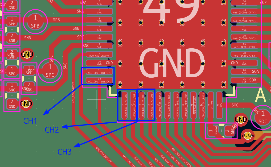
To verify the Timer 1 configuration I used my SIGLENT SDS 1102CML+ Oscilloscope to measure the timer outputs. Below are the probe points for the different Timer 1 channels shown in the PCB design.
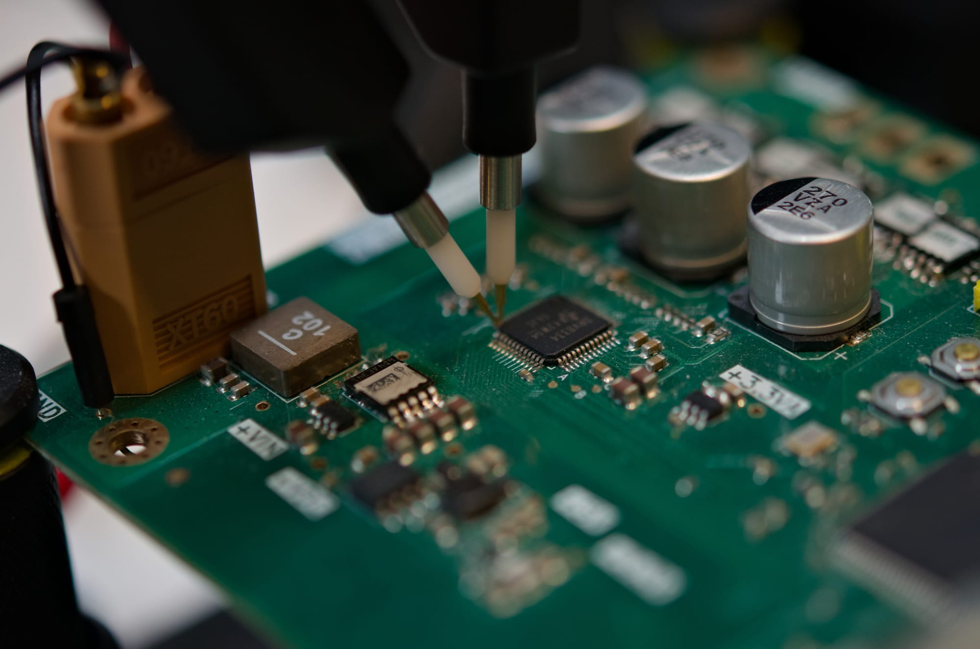
Here we can see the actual probing setup. I quite like the PCBite probes for this purpose, since they make the placement reliable and easy even for small pitched ICs.
Frequency Check
The first measurement revealed that I did mess some thing up for Timer 1 configuration. I measured $40\,kHz$ instead of the expected $20\,kHz$ as seen in the plot below
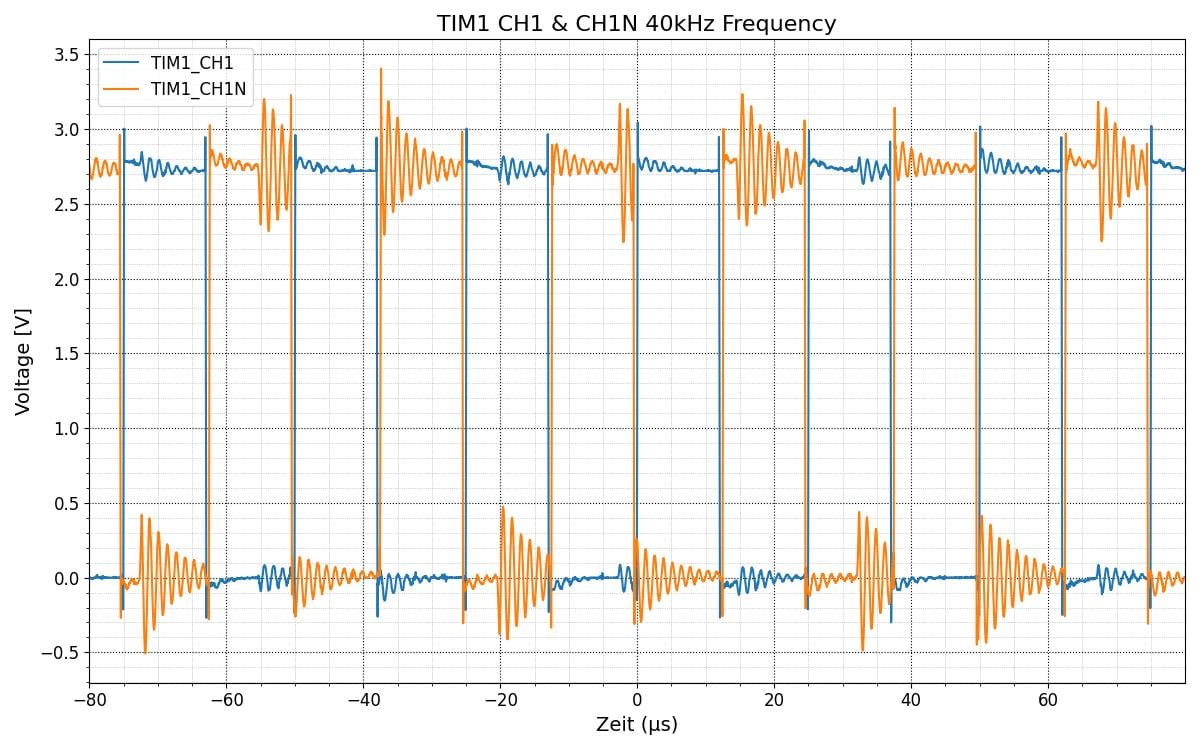
The intial ARR was set to 3000 ticks while the input clock frequncy was set to $120\,MHz$. Due to the up and down counting mode the clock ticks per period are doubled from the usual period calculation, resulting in this equation
$$ \text{Total Clock Ticks Per Period} = 2 \times \text{ARR}$$ With the correct formula the PWM frequency can be calculated like this
$$\text{PWM Frequency} = \frac{f_{\text{CK\_INT}}}{2 \times (\text{PSC} + 1) \times \text{ARR}}$$ Using the initial configuration with PSC=0 and ARR=3000 makes the mistake apparent, resulting in a PWM frequncy of
$$\text{PWM Frequency} = \frac{120\,MHz}{2 \times (0 + 1) \times 3000 } = 40\,kHz$$ By changing the ARR to 6000 this issue should be resolved
$$ \text{PWM Frequency} = \frac{120\,MHz}{2 \times (0 + 1) \times 6000 } = 20\,kHz$$ and can be confirmed by the measurement below
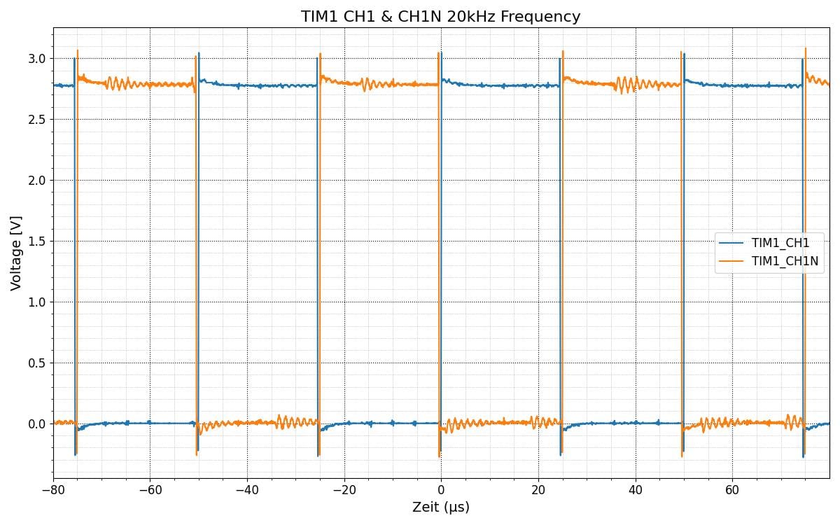
Perfect! I also verified the other two Channels and their complementary parts with the Oscilloscope. Sadly there is no plot, so you have to trust me on that ;).
Center aligned mode
Next I wanted to verify that the PWMs are really configured in center aligned mode. This time I measured CH1 and CH2 of Timer 1 and set the compare value to 2000 and 3000
LL_TIM_OC_SetCompareCH1(tim1, 3000);
LL_TIM_OC_SetCompareCH2(tim1, 2000);
This effectively generates one signal with a $\frac{3000}{6000} \cdot 100 = 50\,\%$ dutycyle and one with $\frac{2000}{6000} \cdot 100 = 33.33\,\%$. This and the center aligned characteristic can be seen quite nicely in the following plot
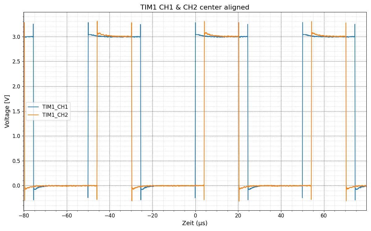
Awesome this is also confirmed to be working.
Deadtime
The last thing to verify for the Timer was the dead time insertion. The configuration of the dead time generator (DTG) can be seen below and is set to a value of DTG=120
================ TIM1 Register Dump ================
Base Address : 0x40010000
----------------------------------------------------
CR1          : 0x000000E1 (CEN=1, CMS=3)
CR2          : 0x00000000
SMCR         : 0x00000000
DIER         : 0x00000000
SR           : 0x0003001F (UIF=1, BIF=0)
EGR          : 0x00000000
CCMR1        : 0x00006868 (OC1M=6, OC2M=6)
CCMR2        : 0x00000068 (OC3M=6)
CCER         : 0x00000555 (CC1E=1, CC1NE=1, CC2E=1, CC2NE=1, CC3E=1, CC3NE=1)
CNT          : 2587 (0x00000A13)
PSC          : 0
ARR          : 3000
CCR1         : 1500
CCR2         : 1500
CCR3         : 1500
BDTR         : 0x0000C078 (MOE=1, AOE=1, DTG=120)
====================================================
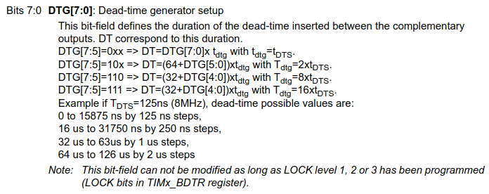
With this setting and a $240\,MHz$ timer clock frequency (CL_INT) this results in a dead time of $$ \text{t}_{\text{dt}} = \text{DTG} \times \text{t}_{\text{DTS}} = 120 \cdot \frac{1}{240\,MHz} = 500\,ns$$ Maybe a higher dead time would be better for testing but I will have to tweak this later anyway or maybe even remove it. Here is the description from the STM32 Reference Manual RM0008 for the DTGRegister
Here is the measurement for the dead time of the complementary PWM signals of Channel 1.
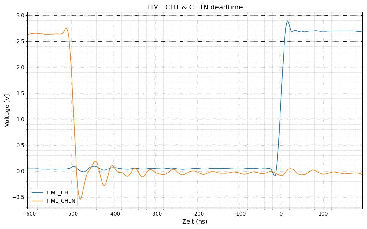
This is in line with what we configured and with this we can move on to the next peripheral to configure.
ADC Setup
The STM32H750VB has three 16-bit ADC, which results in theoretical $2^{16} = 16384$ quantization steps. At a reference voltage of 3.3\,V each least significant bit represents roughly $\frac{3.3\,V}{16384\,LSB -1} \approx 50\,uV$ of resolution. Due to noise and other imperfections along the signal chain the real achievable resolution will be reduced.
These converters operate using successive approximation register architecture supporting high speed conversion rates while maintaining high precision, which is perfect for the application.
The Idea for the ADC is to use the overflow event of the Timer 1 to start all three ADC measurements (one for each of the phases).
I struggled quite a bit here, since I was also not able to utilize the zephyr API due to my requirements. Than I ran into an issue where one of the ADC readings was always of.
uart:~$ read_pb0_avg
==========================================
       ADC1 READ REPORT (16x AVG)
==========================================
ADC1->CFGR Register : 0x80001000
Last ADC1->DR Read  : 49555 (0xC193)
16x Averaged Raw    : 49592 (0xC1B8)
Calculated Voltage  : 2497 mV
==========================================
This value should be around $\frac{3.3\,V}{2}= 1.65\,V$. After a lot of troubleshooting, I figured out that it was due to this ADC being configured in differential mode:
[DIFFERENTIAL & CALIBRATION]
  DIFSEL    : 0x00000200
Changing this to single ended mode resolved this issue.
Now I need to configure the external trigger to the Timer 1. First lets do this with an ISR to check that it is working and move to a DMA method to store the values in RAM.
After that was working for the ADC1 I implemented this for the ADC2 and ADC3 as well.
/* Force Single Ended mode on selected channel */
    if (channel < 32)
    {
        instance->DIFSEL &= ~(1U << channel);
    }

    /* 3. Configure ADC Instance */
    hadc->Instance = instance;
    hadc->Init.ClockPrescaler = ADC_CLOCK_SYNC_PCLK_DIV4;
    hadc->Init.Resolution = ADC_RESOLUTION_16B;
    hadc->Init.ScanConvMode = ADC_SCAN_DISABLE;
    hadc->Init.EOCSelection = ADC_EOC_SINGLE_CONV;
    hadc->Init.LowPowerAutoWait = DISABLE;
    hadc->Init.ContinuousConvMode = DISABLE;
    hadc->Init.NbrOfConversion = 1;
    hadc->Init.DiscontinuousConvMode = DISABLE;

    hadc->Init.ExternalTrigConv = ADC_EXTERNALTRIG_T1_TRGO;
    hadc->Init.ExternalTrigConvEdge = ADC_EXTERNALTRIGCONVEDGE_RISING;

    hadc->Init.ConversionDataManagement = ADC_CONVERSIONDATA_DMA_CIRCULAR;
    hadc->Init.Overrun = ADC_OVR_DATA_OVERWRITTEN;
    hadc->Init.OversamplingMode = DISABLE;

    if (HAL_ADC_Init(hadc) != HAL_OK)
    {
        return -1;
    }

    hadc->Instance->CR &= ~ADC_CR_DEEPPWD; /* Exit Deep Power Down */
    hadc->Instance->CR |= ADC_CR_ADVREGEN; /* Enable ADC Internal Regulator */

    /* Wait for LDO startup time */
    k_busy_wait(20);

    /* 4. Voltage Regulator and Calibration */
    if (HAL_ADCEx_Calibration_Start(hadc, ADC_CALIB_OFFSET, ADC_SINGLE_ENDED) != HAL_OK)
    {
        return -2;
    }

    /* 5. Channel Configuration */
    ADC_ChannelConfTypeDef sConfig = {0};
    sConfig.Channel = channel;
    sConfig.Rank = ADC_REGULAR_RANK_1;
    sConfig.SamplingTime = ADC_SAMPLETIME_32CYCLES_5;
    sConfig.OffsetNumber = ADC_OFFSET_NONE;
    sConfig.SingleDiff = ADC_SINGLE_ENDED;
Offset Calibration
For offset calibration, the system collects multiple background readings during startup, calculates their mean, and stores this value as a fixed offset factor to subtract from future measurements. Averaging $32$ samples at a sampling rate of $20 \, kHz$ takes $1.6\, ms$, calculated as $\frac{1}{20\,kHz} \cdot 32 = 1.6\,ms$. Assuming uncorrelated Gaussian noise, taking $N = 32$ samples reduces the random noise standard deviation by a factor of $\sqrt{32} \approx 5.66$, which is equivalent to $10 \cdot \log_{10}(32) \approx 15.05\,dB$.
Sampling 64 samples for Phase A, B, C current offset...
==========================================
     CURRENT OFFSET CALIBRATION SUCCESS
==========================================
Phase A Offset : 32840 raw (1653 mV)
Phase B Offset : 32719 raw (1647 mV)
Phase C Offset : 32919 raw (1657 mV)
==========================================
Noise Measurement
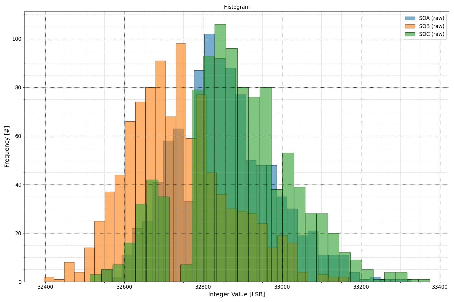
Now since the basic ADC function is working, I would like to know how good the ADC performance is. To analyse the noise performance of the whole system (remember this measures the whole chain from the Shunt to the CSA of the GDU through the input filter of the ADC and the ADC itself), I created shell command function that takes $1000$ measurement and prints them in a .csv compatible format to the output. Using that as an input I did some basic noise calculations for each of the ADCs
- Mean value: $\bar{x} = \frac{1}{N} \cdot \sum_{i=1}^{N} x_i$
- Standard deviation: $s = \sqrt{\frac{1}{N - 1} \cdot \sum_{i=1}^{N} (x_i - \bar{x})^2}$
- Min: $x_{min} = \min(x_1, x_2, \dots, x_N)$
- Max: $x_{max} = \max(x_1, x_2, \dots, x_N)$
- Delta: $\Delta x = x_{max} - x_{min}$
The histogram for all three ADC measurements can be seen below
and the noise parameters are shown in this image
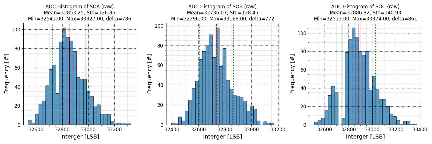
From these plots we can see that Phase B has a slightly lower offset than the other two channels. The deviations are all around the same with a delta of around 820\pm 50\,LSB and a standard deviation of $\sigma = 135 \pm 5\,LSB$. Other noteworthy detail is that neither of the ADC shows a smooth bell curve. Also on phase C there seems to be some Missing Codes at $\approx 32700\,LSB$. Nonetheless overall this should be sufficient for the application.
Ideally I would have like to also verify that the Timer and ADC are triggering the way I specified in the beginning, but sadly I do not have the equipment to measure this. I would need at least a oscilloscope with 4 channels. Then I could route the trigger for the ADC to an GPIO pin and measure the trigger point. On the second channel I could show the Current Sense Amplifier output that is fed into the ADC and on the third channel I could show the timer signal outputs. I might do that in another blog post in the future.
Conclusion
The successful configuration of Timer 1 and synchronized ADC triggering establishes a stable foundation for closed loop motor control. Verifying the timing parameters, dead time insertion, and noise characteristics ensures that phase current measurements remain accurate and reliable under operation.
This concludes the second part of this series. I am looking forward to the next parts. Happy patching!