DIY Motor Controller Part I: Hardware Design & Bringup
Intro
Ever since I learned about motors and control systems at university, I have wanted to build a controller from scratch. I enjoy bringing theory to life, with the long term goal of using these controllers in a custom robotics system in the future. Having worked on the hardware side of three phase motor controllers at a previous employer, I had a good idea of the key hardware requirements. On the Firmware development side I was not deeply involved, therefor this will be a new area for me to explore. The hard part will be the firmware development to replicate my ideas. This will be a multi part series, as I cannot compress everything into a single post. I will update the outline below with links as new posts are released:
- Hardware Design & Bringup (TBD)
- Firmware: Timer & ADC Configuration (TBD)
- Firmware: BLDC Intro & GDU Configruation (TBD)
- Firmware: Simulation & Open Loop Control (TBD)
- Side Quest: External Flash & XiP (TBD)
- Firmware: Closed Loop Control (TBD)
- Side quests (TBD)
Without further ado lets dive into the hardware design process.
Requirements/Goals
As any good engineer would do, I start with a rough sketch on what my desired requirements are and what the purpose of this project is going to be. (I swear I did not write this afterwards). The main goal is to build and program a working prototype for a BLDC motor controller from scratch. Later on we can add some more of the fancy stuff, if I get the time for that. I am also pretty sure that there will be some mistake along the way, but that is what learning requires. Also where is the fun in everything going according to plan.
List
- Input voltage range: $0-28,V$ ($24,V$ nominal)
- Current: up to $100,A_{peak}$ ($70,A_{peak}$ nominal)
- Operating temperature of max $-20\,°C$ to $80\,°C$
- TI Gate Driver Unit (GDU)
- STM32 MCU
- Zephyr RTOS for firmware development
- 2x Can Interfaces for communication
- 1x Ethernet ($100\,MBit$)
- Motor Position Sensor (MPS)
- some spare GPIOs
- Debugging via TC-2050 cable (I think I will have to do a blog post about this in the near future)
- Target Motor is a BLDC Motor - Turnigy Aerodrive SK3 5055 430kV (I already have them lying around)
The primary voltage will be $12\,V$ but I also want to have the option for some more power output, thats why I target a higher voltage in the design as well. Also this will allow a wide range of input options (different battery configurations and so on).
$100\,A$ is a nice number
Normal operation condition nothing fancy
For the MCU STM should have some good options and I am used to programming them. Mainly the standard STM32F103 and STM32F405 types so far.
Similar to the MCU, I am familiar with Zephyr RTOS, which fits well here.
For the communication CAN should be quite robust and also chainable. Not sure how good this will be in case of multiple controller being on the same Interface, but that is an issue for the future Paul. For the Ethernet I would like to test this and maybe dive into Real-Time-Ethernet for control purposes. In general, ethernet will become relevant when connecting multiple controllers into a single system (such as a robotic platform).
For the MPS I already did make a design see and a blog post about it: Motor Position Sensor (MPS). So I want to integrate this here and use it
This should cover the most basic requirements for the system. At least I think that with this I should be able to cover a wide range of options in the future.
Hardware Deep Dive
Gate Drive Unit (GDU)
Lets first decide on the main part and make the selection of the MCU dependent on the GDU and what it requires. For the GDU I settled on the integrated Drive Unit DRV8334 which has the following features:
- SPI up to $10\,MHz$
- 6x PWM inputs (independent)
- 3x Current Sense Amplifier outputs
- 2x GPO for
SLEEPandDRVOFF - 1x GPI for
FAULTdetection VREF: $3.3\,V$ / $5\,V$- Gain settings: 5 up to 40
MCU
Initially, I planned to use an STM32G474RE , but later settled on an STM32H750VBbecause I wanted to evaluate a high end STM32 MCU. The STM32G474RE would also have been a fine choice especially with its CORDIC accelerator and more ADC units. The main reason for the STM32H750VB was the Ehternet support that the STM32G474 lacks.
For both the advanced timer 1 will be used to generate the PWM signal for the GDU control. Both microcontrollers feature at least three ADC units, enabling simultaneous sampling of three phase currents. In this case I intend to sample the current measurements at the same time.
Another thing that I considered here is that the STM32H750VB only has $128\,kbyte$ of on-board flash memory. Therefore I added a $128\,Mbit$ external flash in the form of the W25Q128JV. I will have to later figure out how to boot from the external flash, I never have done that before. Paul of the future here: This is a lot more work than I anticipated, just have to learn something new!
Reverse Polarity Protection (RPP)
To protect the board from potential mishandling by an inexperienced engineer (namely myself), I will be adding a N-Channel based Reverse Polarity Protection. For this I will be utilizing a LM74700, that has a built in charge pump to supply the needed voltage to turn the MOSFET on. I went with the default recommended values and did use the same MOSFET as for the 3 phase bridge. Fun Fact: I could have used the TCP pin of the GDU instead of the LM74700. This would have been cost and space efficient.
Power Regulators
To supply all the selected components the following voltage rails are needed:
- Input voltage to $5.0\,V$ buck converter
- $5.0\,V$ to $3.3\,V$ buck converter
- $3.3\,V$ LDO for low noise analog power
TPS5405 (5.0V)
External component selection:
Expected maximum output is $1\,A$ , with a nominal operating current closer to $500\,mA$. I will go with the highest switching fequency of $1.2\,MHz$ and configure the ROSC to floating.
$0.1\,uF$ for BOOT and LX pins
$10\,nF$ for the slow start pin results in
$$t_{ss} = \frac{C_{ss}\cdot V_{ref}}{I_{ss}} \quad \mathrm{with} \quad I_{ss}=2,\mu A \quad V_{ref}=0.8,V \Rightarrow \frac{10,nF \cdot 0.8,V}{2,\mu A} = 4\,ms$$
softstart time.
Inductor Selection
With the provided equation from the datasheet
$$L = \frac{V_{IN} - V_{OUT}}{I_{OUT} \cdot LIR} \cdot \frac{V_{OUT}}{V_{IN} \cdot f_{SW}}$$
and the desired output voltage $V_{OUT} = 5,V$ and the input range of $V_{IN} = 12,V$ to $24,V$ this results in
$$L = \frac{5,V - 12,V}{1,A \cdot 0.2} \cdot \frac{5,V}{12,V \cdot 1.1,MHz} = 10\,uH$$
The actual component I will use for the inductor is SWPA6028S100MT.
Output Capacitor Selection
The target ripple voltage is
$$10\% \Rightarrow 5,V \cdot 10\% = 500\,mV$$
and the current transient is $\Delta A = 1\,A - 0\,A = 1\,A.$
$$C_{OUT} > \frac{\Delta I_{OUT}^2 \cdot L}{2\cdot V_{OUT} \cdot \Delta V_{OUT}} = \frac{(1,A)^2 \cdot 10,uH}{2 \cdot 5,V \cdot 0.5,V} = 2 ,uF$$
Selection of $3\times 10\,uF$ (CL10A106MA8NR) with an ESR around $4.5,m\Omega$ each rated for $10\,V$ (derating to $\approx 50\%$ at $5.0\,V$)
TPS62A01AD (3.3V)
Feedack divider
The device needs a feedback divider to configure the output voltage. Since we want $V_{OUT}=3.3\,V$, I calcualted the required resistor values with the formula from the datasheet
$$R_1 = R_2 \cdot \left(\frac{V_{OUT}}{V_{FB}} - 1\right) \Rightarrow 47\,k\Omega \cdot \left( \frac{3.3\,V}{0.6\,V} -1\right) = 211.5\,k\Omega \approx 200\,k\Omega$$
TPS7A0333 (3.3V)
For the ADC measurement the TPS7A0333 will be used to supply a low noise $3.3\,V$ signal, that will be used by the GDU, the MCU and the Temperature sensor as a reference.
This device support up to $200\,mA$, which provides ample margin for my design. For this only the input and output capacitors had to be $10\,uF$ according to the datasheet.
Motor position sensor type
For details on this part see my separate blog post Motor Position Sensor (MPS). I basically just need a $3.3\,V$ or $5\,V$ supply and the desired interface pins. For this prototype, I am bringing out all available interface options, including SPI and ABI (incremental encoder) timer inputs. Back-EMF sensing could also provide sensorless position estimation. However, that is planned for Revision 2 and is outside the scope of this initial prototype. I believe this requires a floating reference star point.
MOSFETs
The main component that decides what kind of power we can switch is the MOSFET. Having interned at Infineon, and considering their position as a leading European semiconductor manufacturer, I chose Infineon MOSFETs for the power stage. Based on the system requirements. I was looking for something with these parameters:
- $V_{DS} = 30-40\,V$
- $I_D \geq 100\,A$
- Cooling via top side. Usually the MOSFETs are cooled by connecting them to the PCB with a copper pour, but I wanted to try something different. I know that this requirements limits the component selection quite heavily, but I wanted to try this.
After some searching around I settled on the IAUCN04S6N017TATMA1, which might be a little bit overkill for my purpose but hey this is a prototype and maybe we can have some fun with this later on. An important parameter is the total gate charge ($Q_{g,typ.} = 38\,nC$). Together with the peak drive current of the GDU, this determines the switching speed.
For cooling I would like to later use
- Thermal interface material (TIM - not to be confused with the abbreviation for Timer, which is also TIM :) ) -> use precut sheets here
- Cooling Heatsinks
NTC Temperature Sensor
To allow monitoring the MOSFET temperature I will be adding a NTC close one of the MOSFETs. The specific NTC used is the NTCS0603E3103FLT, which is a $10\,k\Omega$ NTC.
DC Link Capacitors
These provides the main power for the 3 phase switching and need to be sized accordingly. I decided to use 1 Capacitor for each of the phases and landed on the EEH-ZA1V271V/P.
In general for this application you want to have a high capacitance with low ESR Capacitor. Also the ripple current is relevant to ensure a high lifetime of the parts.
Communication
Ethernet
There are no special requirements on my side. I just looked at the supported IC for zephyr and find the LAN8720A, which should do the job just fine. It requires an external $25\,MHz$ crystal and a RJ45 connector with integrated Magnetics (could also be a separate part but makes designing a bit more confident).
CAN Interface
For the CAN I use the TJA1043T and two 4-Pin connectors to allow easy daisy chaining in the future. Also nothing fancy happen here, apart from this requiring a $5\,V$ supply voltage. This is fine for a prototype but ideally I would like to not need an additional power rail for just this use case. In a final design this might be optimizable.
Motor Specifications
Here is a full list of the provided data of the used BLDC Motor:
Electrical
- Umdrehungen: $12\,\text{T}$
- Kv (rpm / v): $430\,\frac{\text{rpm}}{\text{V}}$
- Max Current: $70\,\text{A}$
- Widerstand: $1750\,\text{m}\Omega$
- Max Spannung: $30\,\text{V}$
- Leistung: $1750\,\text{W}$
Mechanical
- Welle A: $6\,\text{mm}$
- Länge B: $59\,\text{mm}$
- Durchmesser $C: 50\,\text{mm}$
- Kann Länge D: $55\,\text{mm}$
- Gesamtlänge E: $80\,\text{mm}$
- Gewicht: $0.378\,\text{kg}$
- Bolzengewinde:
M4 - Motorstecker: $4\,\text{mm} Rundstecker$
Schematic Design
The Schematic was designed in KiCAD and the design can be found on my github repo: https://github.com/Nightshadow1258/HW_Motor_Controller. The Documentation folder contains a pdf version of the Schematic as well and some other interesting bits of information. Here is a high level overview diagram of the components and the connections.
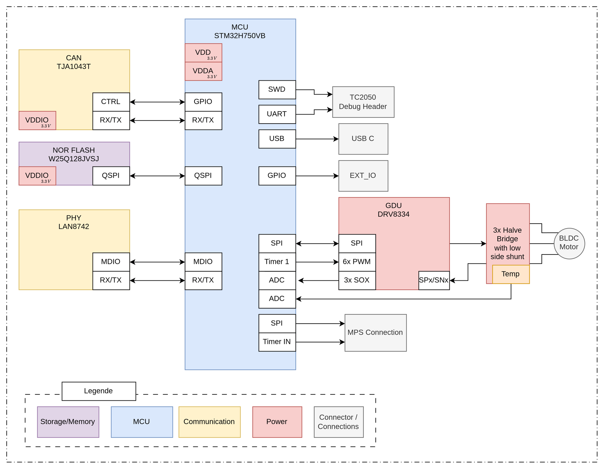
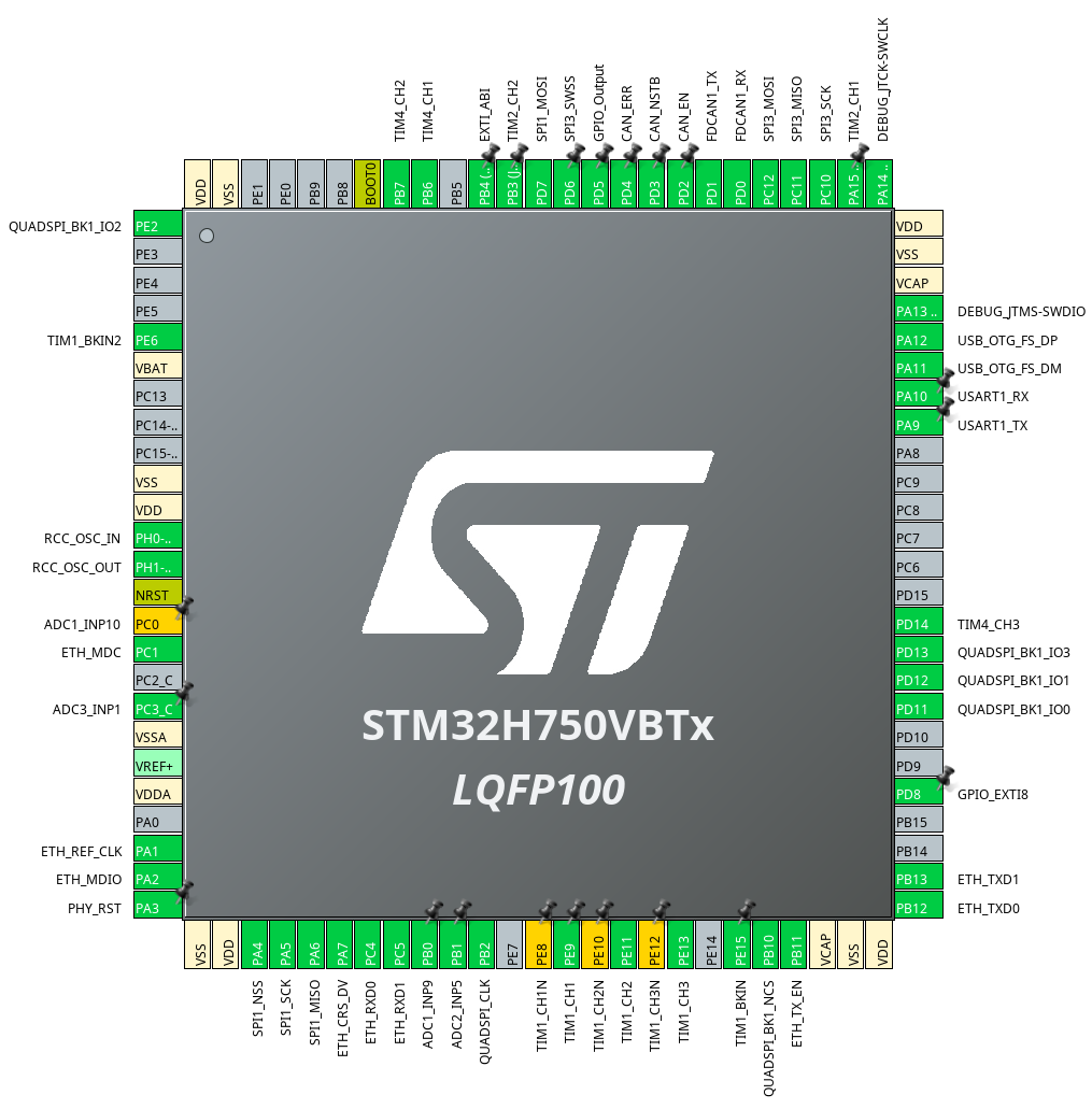
During this process I like to use the STM32CubeMX Software to checkout which pin allows what configuration. I usually start by enabling all required peripherals and then optimize the pin assignment to simplify PCB routing. Here is the final pin configuration that I decided on in the end
PCB Design
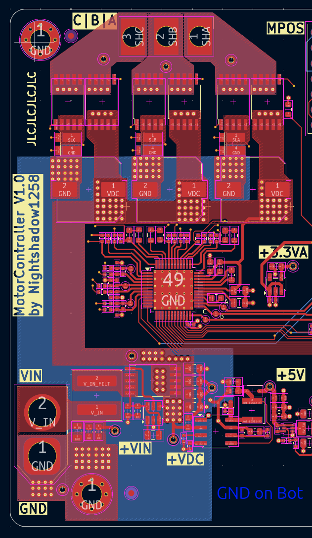
Since this is a high power design with high currents flowing the PCB Stackup has to be considered. Also the high current loops area should be as small as possible to avoid interference due to electromagnetic coupling.
I selected a 2 oz outer copper layer thickness to increase current carrying capacity. I used wide traces and heavy copper pours on these layers for the high power paths. I also separated the board into a high power domain and a digital and analog domain. See the image below for the high power domain. The Bottom Layer is used for the GND and on the TOP layer the VDC is routed. Fun fact I just noticed that I made an oopsie on the cooper pours after the Reverse Polarity MOSFET. This also could be improved in a second revision. The via placement severely restricts the effective trace width on the power rail feeding the DC link capacitors. Letus just say this intentionally increases parasitic resistance to make the capacitors work more efficent! :)
Another important consideration is that the LAN8742 Ethernet PHY requires $100\,\Omega$ differential impedance for the RX and TX lines to the RJ45 connector. Since this is only going to be a $100\,MBit$ link this is not as critical but should still be considered during the routing. This concludes the design process.
PCBs
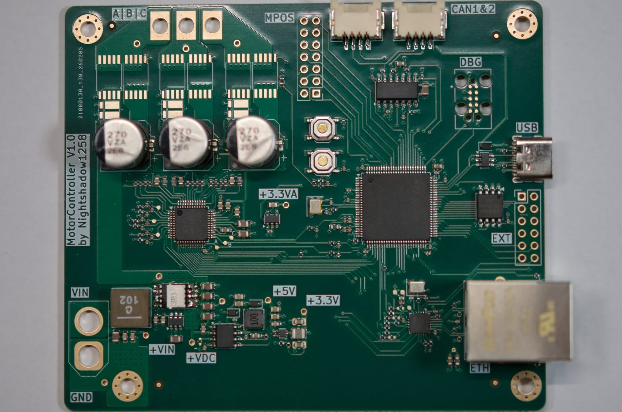
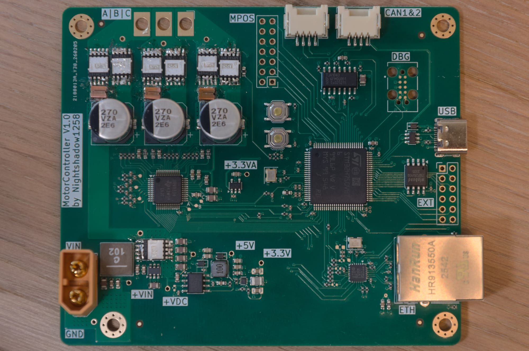
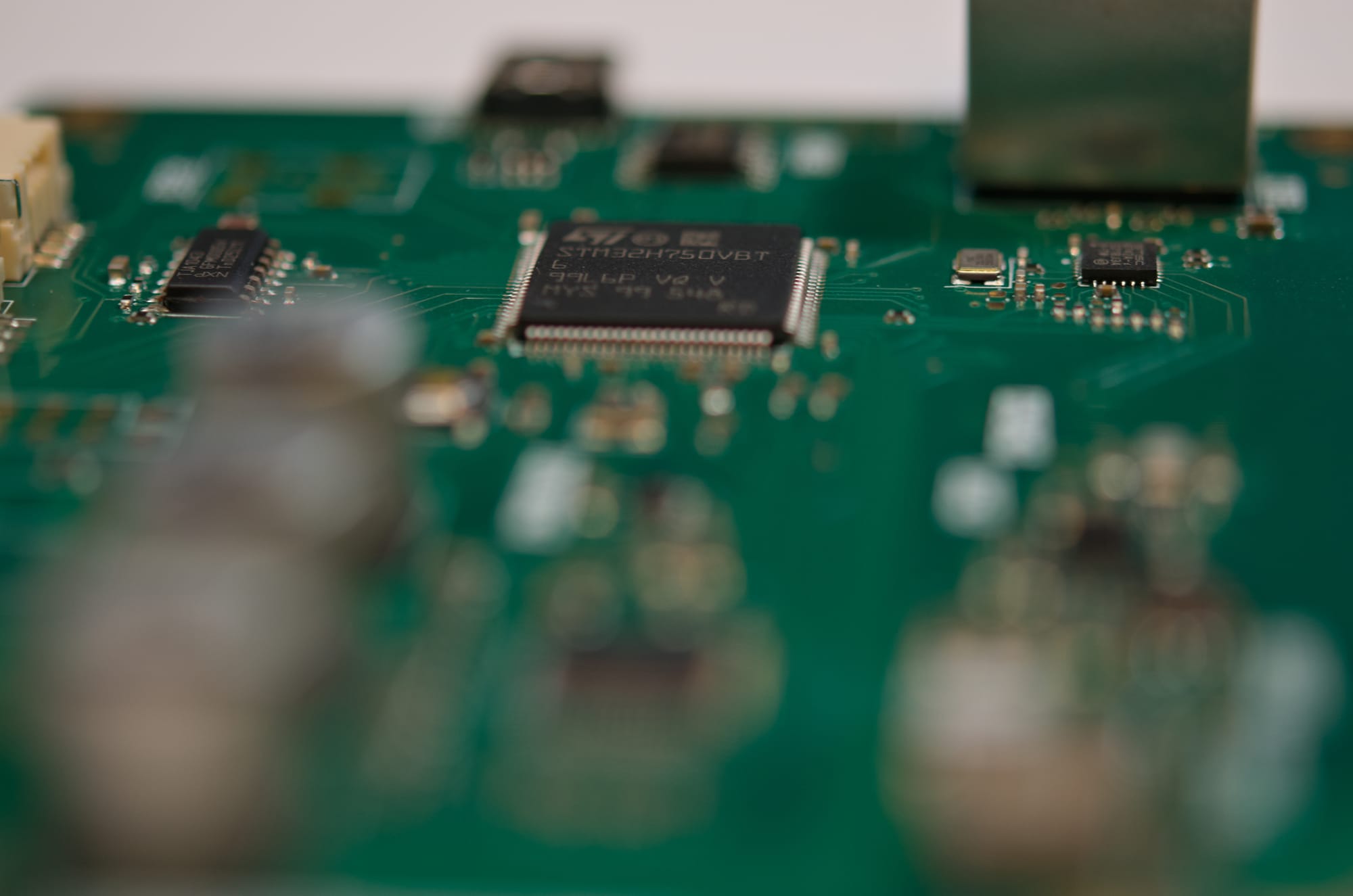
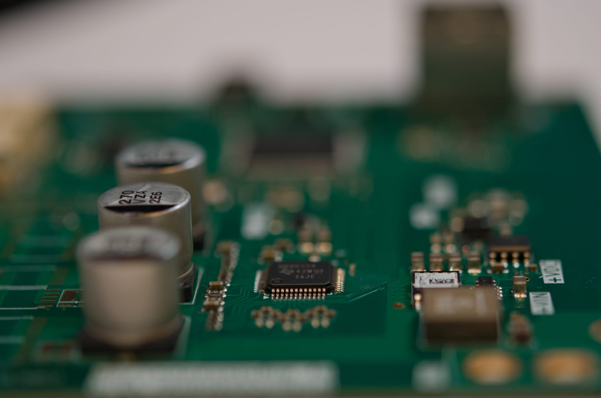
Here it is with the Shunts and the MOSFETs populated. I know not my finest work but damn the copper pours sipped the heat away, making this not so easy. I had to use the heatgun and the soldering iron in tandem to make this work at all. The capacitors were wrapped in Kapton tape to isolate them from the heat.
Bring Up Testing
After inspecting the PCBs and populating the MOSFETs and shunts I did a continuity test on all of the power rails to verify that nothing was shorted. After connection the borad to power I measured the output voltages and notices that the $3.3\,V$ analog supply does not work for some reason. To make sure I also checked with a second board. After some further testing and looking at schematic, layout and datasheet it turns out that I swapped the pin 4 and 5. See the Schematic symbol here
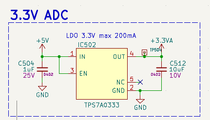
vs the datasheet pinout:
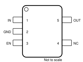
Luckily Pin 5 is a no connect (NC) Pin. The fix was to just short the both pin. Now all the power rails are working and the MCU connects via the debugger! This concludes the first part of this series I am looking forward to the next parts. Happy patching!