Stepper Controller V1.0
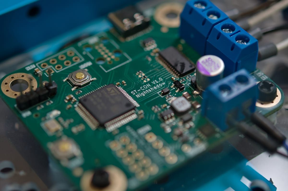
Project information
The main purpose of this project is to get a better understanding on motor controller design. In addition I needed a system to control a stepper with good precision for the Motor Position Sensor (MPS) V1.0 calibration process. Therefore the hardware should not be too complex and not too difficult to control. For this reason I am going to select a GDU with built-in current control, but lets first define some basic requirements for the project.
Requirements
- Input voltage:
12Vto24V(absolute max25V) - Input current:
5A(8Apeak) - MCU STM32F405
- GDU allows driving either 1xStepper or 2xDC Motors
- Reverse Polarity Protection (RPP)
- Interface for wireless communication (initially created for NRF24L01)
- Additional I/O for general purpose use as well
- Mix of development board and highly custom-build board
Driver Selection
Candidates:
- TMC2240: Optimized for stepper control and not really suitable for standard DC motor control.
- DRV8424P: Newer version of the DRV8835 with integrated current sensing and capability up to 35V. This is our guy.
- DRV8835: Max 11V input voltage, which makes it not suitable.
Nice after the selection of the GDU, lets have a deeper look at its features and what I will have to consider during the development process.
DRV8424P In-Depth Analysis
Pinout
I like to start by looking at the pin out of the IC. This already reveals some functionality through the pin description. See the datasheet for the DRV8424E/P on page 5 to 6 for the full list. Here are the
VREFA&VREFB:VCP:ADECAY&BDECAY:TOFF: Configures the constant off-time for decay modes via an external resistor connected to ground.AIN1,AIN2&BIN1,BIN2: Pulse-width modulation (PWM) inputs controlling the direction and duty cycle of Phase A and Phase B bridges directly.
VREFx to configure IREG
The current through the motor windings is regulated by an adjustable, off-time PWM current-regulation circuit. When an H-bridge is enabled, current rises through the winding at a rate dependent on the DC voltage, inductance of the winding, and the magnitude of the back EMF present. When the current hits the current regulation threshold, the bridge enters a decay mode (set by ADECAY & BDECAY) for a period of time determined by the TOFF pin setting to decrease the current. The current regulation threshold (IREG) can be set by the VREFx inputs of the IC following the calculation below:
$$V_{REF} = D_{VDD} \cdot \frac{R_1}{R_1 + R_2} = 3.3V \cdot \frac{10\,k\Omega}{10\,k\Omega + 2\,k\Omega} = 2.75\,V$$
$$I_{REG} = \frac{V_{REF}}{1.32} = \frac{2.75\,V}{1.32} = 2.08\,A$$
I will not use a fixed resistor setting, but instead use a DAC output of the MCUs. This allows changing this parameter on the fly, making the application more versatile.
Reverse Polarity Protection with VCP
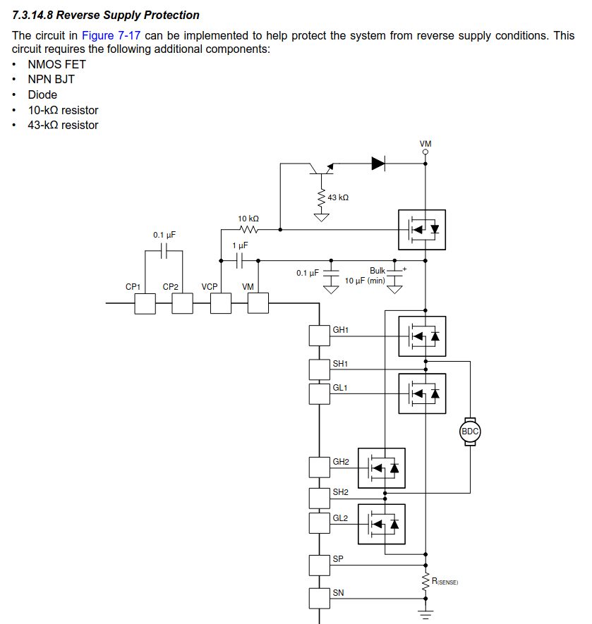
Since there were not details on how to use the VCP an external Reverse Polarity Protection and knowing that this is used in many different TI Drivers, I went looking for a datasheet with an example schematic. I was able to dig up the following configuration from the DRV8702 Datasheet.
This circuit utilizes the internal charge pump of the motor driver (such as the DRV8424P or DRV8702-Q1) to drive an external N-channel MOSFET for reverse supply protection. This method is an efficient alternative to standard Schottky diodes or P-channel MOSFET configurations.
Circuit Architecture and Components
The protection stage is placed between the power supply (VBAT) and the motor driver supply pin (VM). It consists of the following primary elements:
- N-Channel MOSFET (
Q1): Positioned with the Drain toward the supply and the Source toward the load (VM). This orientation ensures the body diode blocks current during a reverse polarity event. - Gate Resistor (
RG): A high-value resistor (typically 10 k\Omega to 100 k\Omega) connects the driver's VCP pin to the MOSFET gate. This limits the inrush current to the gate and protects the internal charge pump from transients. - Zener Diode (DZ): Placed between the Gate and Source of
Q1to clamp V_{GS} to a safe level (e.g., 12V or 15V), preventing gate oxide damage during supply spikes. - NPN Transistor and Signal Diode: These components act as a fast discharge path. During a power loss or a negative transient, the NPN pulls the MOSFET gate to the source potential, ensuring the FET shuts off rapidly to protect downstream components
Theory of Operation
1. Forward Bias (Normal Power-Up) When a positive voltage is applied, current initially flows through the body diode of Q1 to the VM pin. Once the motor driver receives power, it activates its internal charge pump. The VCP pin rises to approximately VM+10V. This voltage is applied to the gate of Q1, turning the MOSFET fully ON. The low $R_{DS(on)}$ of the MOSFET shorts out the body diode, significantly reducing power dissipation and voltage drop.
2. Reverse Bias (Protection Mode) If the supply polarity is reversed, the body diode of Q1 is reverse-biased and blocks current flow. Because the motor driver does not receive power, the VCP pin remains at 0V. The MOSFET gate stays uncharged, keeping Q1 in the OFF state. This effectively isolates the system from the negative voltage.
Design Considerations for Motor Drivers
When using the VCP pin of an integrated driver like the DRV8424P:
- Startup The driver must be able to start via the MOSFET body diode. Ensure the
VMpin can handle the momentary diode drop during the charge pump ramp-up. - Charge Pump Loading: The
VCPpin is designed to drive internal gates. External circuitry must have negligible DC leakage. If theVCPvoltage sags below a specific threshold, the IC may trigger a Charge Pump Undervoltage (CPUV) fault and shut down.
ADECAY & BDECAY
The ADECAY pin sets the decay mode for H-bridge A (AOUT1, AOUT2), and the BDECAY pin sets the decay mode for H-bridge B (BOUT1, BOUT2)
There are the following settings available
| xDEACY | DECAY Mode |
|---|---|
| 0 | Smart tune Dynamic Decay |
| 1 | Smart tune Ripple Control |
| Hi-Z | Mixed decay: 30% fast |
330 \,k\Omega to GND |
Fast decay |
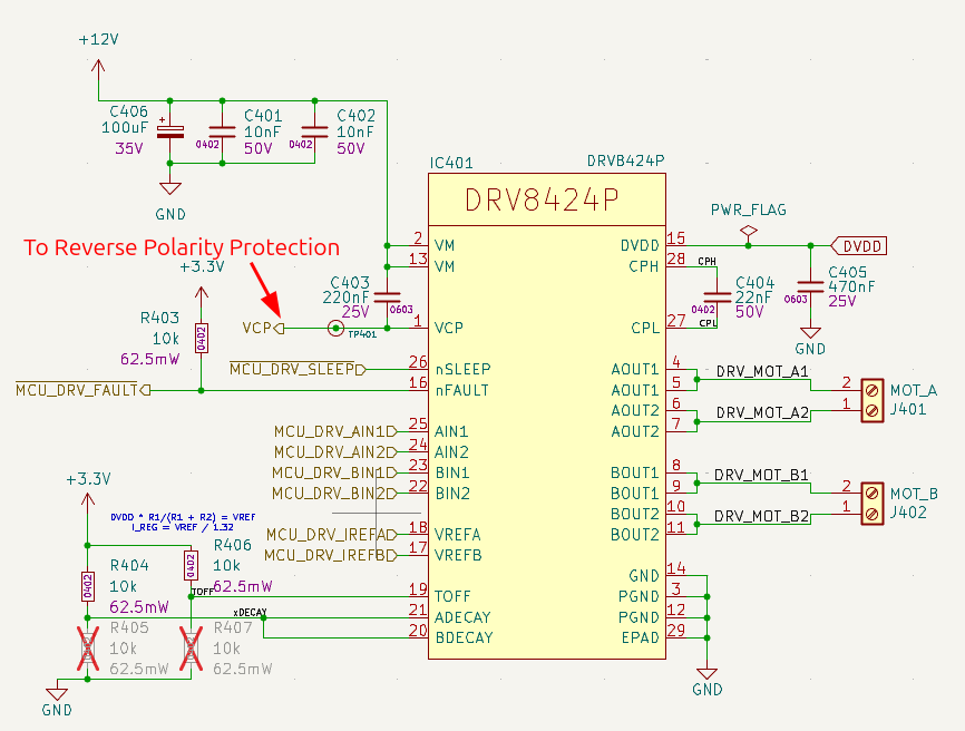
In my design a pulled both xDECAY pin to the 3.3V supply voltage with a 10\,k\Omega resistor. This method allows much tighter regulation of the current level increasing motor efficiency and system performance. Smart tune Ripple Control can be used in systems that can tolerate a variable off-time regulation scheme to achieve small current ripple in the current regulation.
TOFF
Note: Since I am using the Smart tune Ripple Control the TOFF input is ignored. Configures the constant off-time for decay modes via an external resistor connected to ground.
Else the Off time can be configured like so
| TOFF | OFF-Time TOFF |
|---|---|
| 0 | $7\, \mu s$ |
| 1 | $16\, \mu s$ |
| Hi-Z | $24\, \mu s$ |
$330 \,k\Omega$ to GND |
$32\, \mu s$ |
In my design a pulled both TOFF pin to the 3.3V supply voltage with a 10\,k\Omega resistor.
AIN1, AIN2 & BIN1, BIN2
Motor control via PWM enables realtive free control of the motor due to its high configurability in software. The main purposes are going to be
DC Motor Mode
Driving two brushed DC motors requires configuring the input pins to operate as dual independent H-bridges. In this mode, AIN1/AIN2 control Bridge A output, while BIN1/BIN2 control Bridge B. Current limiting remains active per bridge via VREFA and VREFB.
Stepper Motor Mode
When driving a bipolar stepper motor, the inputs act as phase controls for the two windings. Indexer logic or direct PWM feeding AINx and BINx manages phase sequence, while microstepping profile execution relies on scaling VREF dynamically via the MCU DACs.
Schematic Design
The Hardware Design is done in KiCAD and all files can be found here. There is also a pdf export of the Schematic available here
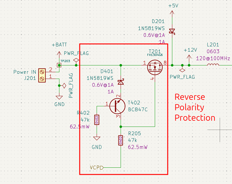
Reverse Polarity Implementation
See below the RPP implementation based on the VCP example schematic design from above.
Layout Design
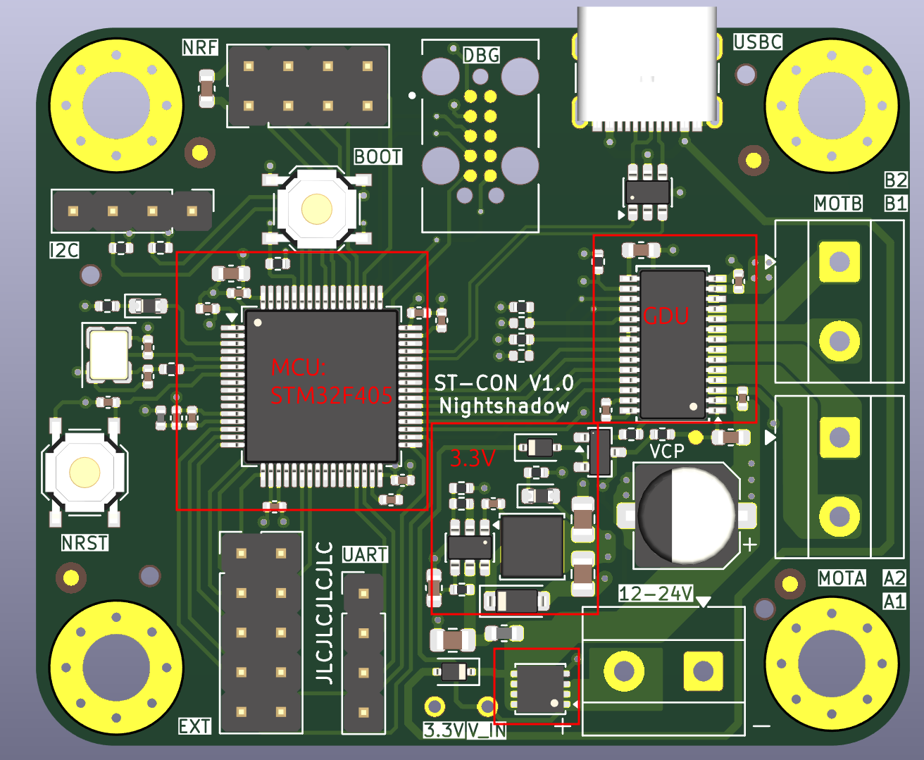
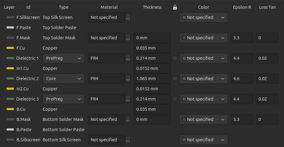
Since 4 Layer PCB are comparable in cost to 2 Layer PCBs these days, I decided to us a 4 layer board. This will also make routing a lot easier and should also improve EMC aspects as well.
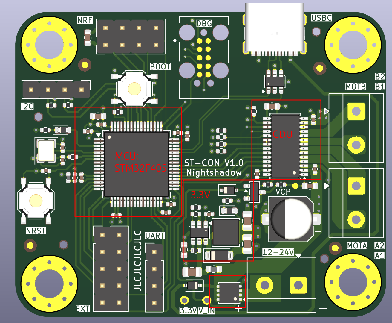
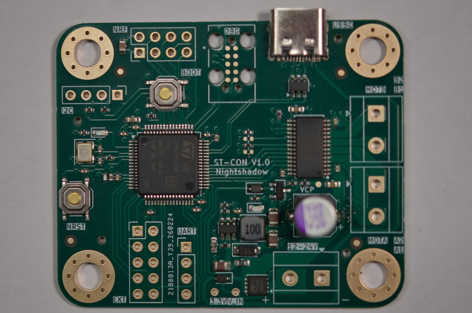
Apart from that only the power traces need some checking. Power traces are routed as thick as possible to handle current limits and to size the power traces for $I_{\text{continuous}} = 5\text{A} (8\text{A} peak)$.
Board Bringup
Before connecting the board I did a quick sanity check that there are no short on the input and GND. I could have verified more but let's risk it and connect the POWER. After nothing release magic smoke I measured the 3.3V voltage rail and confirmed that it is stable with the USB C connected. The power meter shows a current draw below 10mA, which also seems to be fine.
With that I should be able to flash to the MCU to confirm that it is working. For some reasons I had inconsistencies during flashing and connection issuesm though I was able to flash it once. Since I am using a custom adapter that allows be to use the TC-2050 cable to flash the board, I suspected that there is an issue with that.
I basically route the connection from the ST-Link V2.0 debugger and an additional UART converter through to the TC-2050 cable. I checked the connections with the multimeter and did not find any issues. It also tried with the adapter directly connected to the Debug Interface.
The flashing finally consistently worked while using only the four ST-Link V2.0 connections:
- PWR
- GND
- SWCLK
- SWDIO
These were connected to the 20-pin ribbon cable to my custom debug board and then via the TC-2050 cable to the board. So far I only used the USB-C or the 3.3V supply of the debugger to power the board. Therefore next up for testing was the 12V input, which did work, as indicated by the User LED blinking (simple blinky sketch was used during the testing) and the PWR LED also lighting up.
Firmware
There is a link to the Github Repo for this project:
https://github.com/Nightshadow1258/FW_STM32F405_DRV8424P (DRV8424P Stepper Firmware with software-based microstepping and blinking LED thread)
The Firmware is based on zephyr. For the initial Bringup Testing I used a simple blinky sketch to pulse my included User LED on the board.
Since the MCU is now working and is ready to be flashed and used, only the Dual H-bridge motor driver DRV8424P remains to be tested.
First Start with FW for Stepper
5V
- Test case with only USB-C powered by 5V and the debugger connected (STlink & UART)
9V Test
With 9V supplied a little bit of movement is possible but I think that I will need to work on the control algorithm in detail to figure out what to do. I am currently just setting the duty cycle to 100% and set the speed by using a delay that is not so optimal I think. The delay must be configurable to enable ramp up also the duty cycle can probably be reduced during rotation, but this will reduce the torque output as well.
Realization
After a long period of testing and measuring with the Oscilloscope I realized that the GDU on my board was not the correct one. In state I got a DRV8424, which has a slightly different pinout and is only for driving Stepper Motor. See the datasheet here for details. Well classic prototype problem :)
Not that big of an issue I just ordered the actual part that in needed from digikey and in the mean time did a comparison of the pinouts to see if I could also use the DRV8424 in my current Design.
Pin out Comparison Table DRV8424P vs DRV8424
In order to check if I could still make the board work I did a quick comparison the pin of of the two ICs, which can be seen below (thick marked Pins are different between the versions)
| DRV8424P | DRV8424 | ||
|---|---|---|---|
| PIN NAME | PWP PIN NO. | PIN NAME | HTSSOP NO. |
| VCP | 1 | VCP | 1 |
| VM | 2 | VM | 2 |
| PGND | 3 | PGND | 3 |
| AOUT1 | 4 | AOUT1 | 4 |
| AOUT1 | 5 | AOUT1 | 5 |
| AOUT2 | 6 | AOUT2 | 6 |
| AOUT2 | 7 | AOUT2 | 7 |
| BOUT2 | 8 | BOUT2 | 8 |
| BOUT2 | 9 | BOUT2 | 9 |
| BOUT1 | 10 | BOUT1 | 10 |
| BOUT1 | 11 | BOUT1 | 11 |
| PGND | 12 | PGND | 12 |
| VM | 13 | VM | 13 |
| GND | 14 | GND | 14 |
| DVDD | 15 | DVDD | 15 |
| nFAULT | 16 | nFAULT | 16 |
| VREFB | 17 | VREF | 17 |
| VREFA | 18 | M0 | 18 |
| TOFF | 19 | TOFF | 19 |
| BDECAY | 20 | DECAY1 | 20 |
| ADECAY | 21 | DECAY0 | 21 |
| BIN2 | 22 | M1 | 22 |
| BIN1 | 23 | STEP | 23 |
| AIN2 | 24 | DIR | 24 |
| AIN1 | 25 | ENABLE | 25 |
| nSLEEP | 26 | nSLEEP | 26 |
| CPL | 27 | CPL | 27 |
| CPH | 28 | CPH | 28 |
| PAD | — | PAD | — |
Luckily I was able to modify the pins configurations on the MCU to make the Stepper Driver DRV8424 work. For that I created a separate Firmware, which can be found here. The main difference is the stm32f405_stepper.dts, which contain the pin mapping and configuration.
GDU Swap
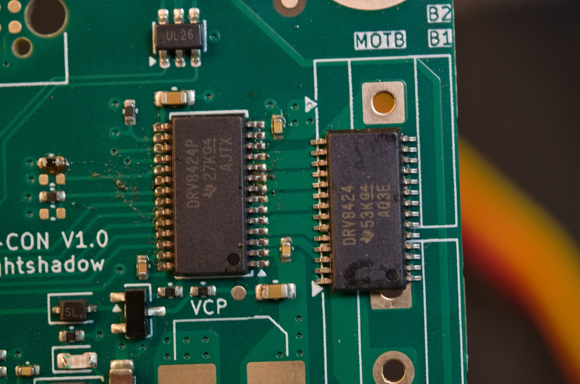
After the replacement IC was delivered I swapped them on one of my boards. Here you can see both IC next to each other. The correct one DRV8424P is now soldered on to the board, while the wrong DRV8424 is lying next to it.
Who would have guess, but after the swap my original Firmware did show the expected behavior! With the correct driver populated, the board is now fully functional.
VCP Measurement
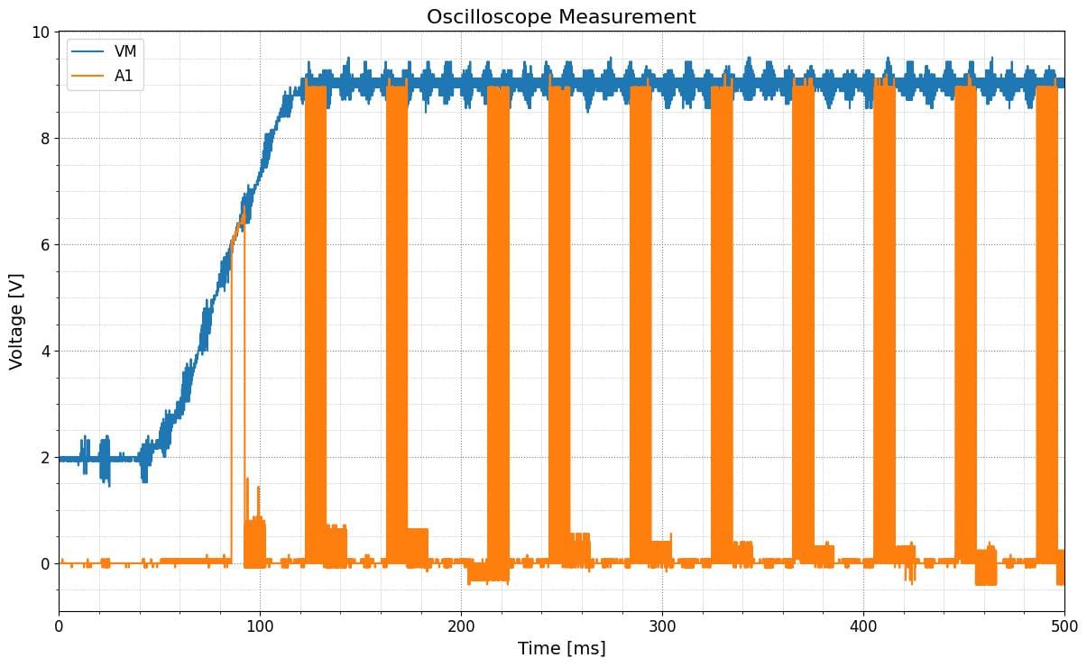
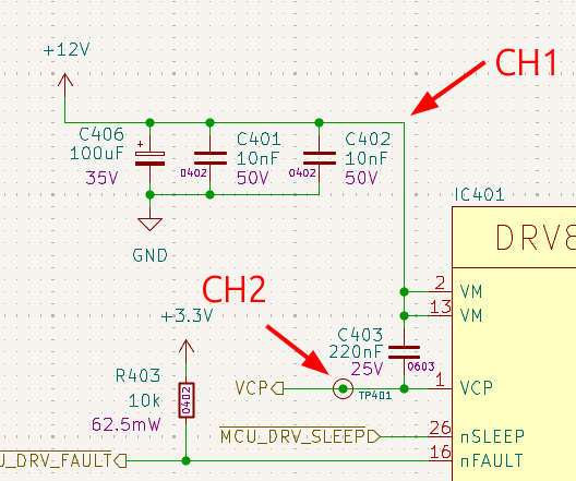
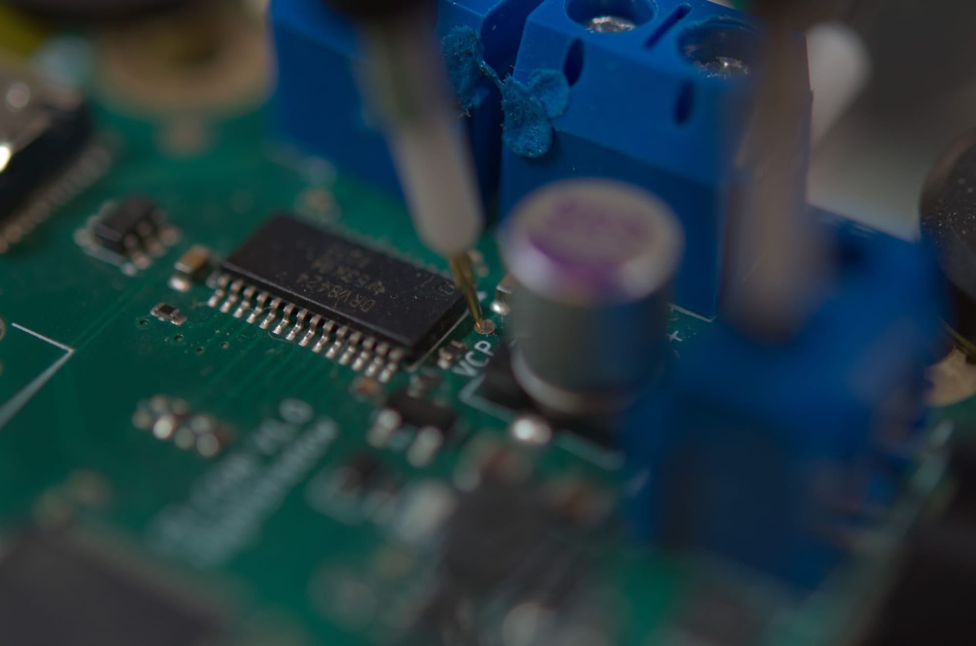
To check if the VCP voltage gets charged up correctly to VM + 5V according to the datasheet. I did a small measurement of the VM and the VCP.
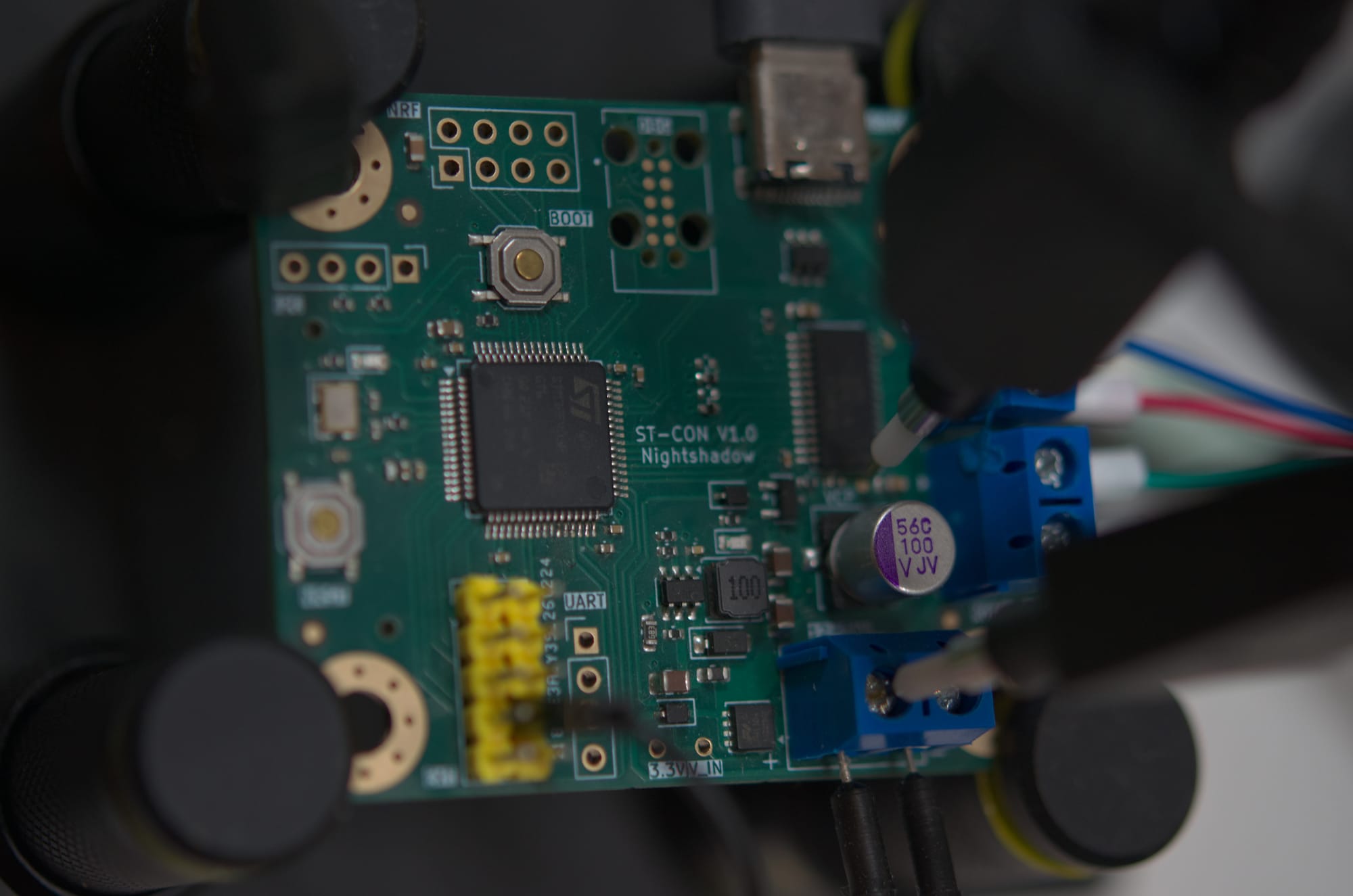
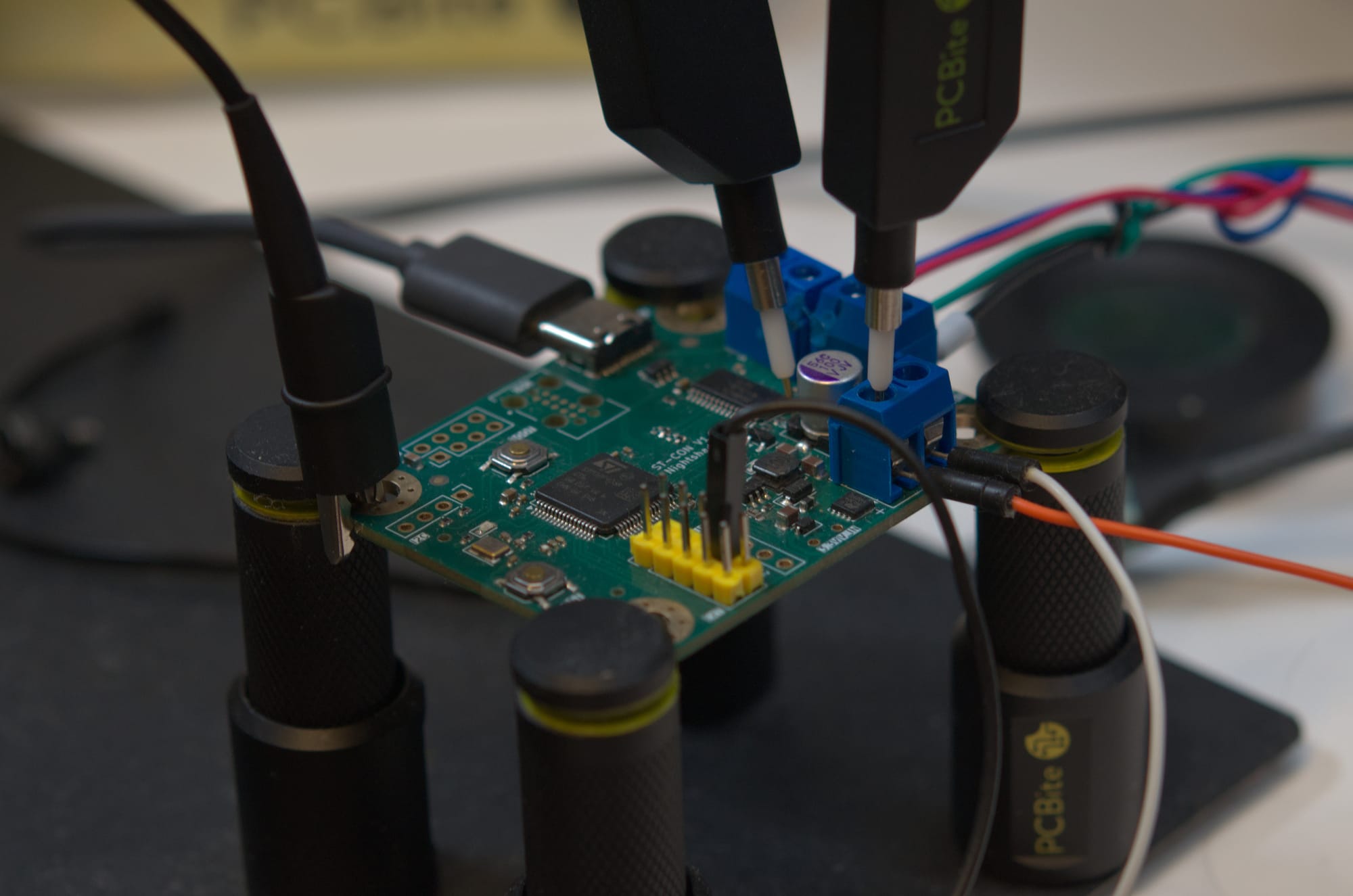
Here are some shots from the the test setup with the PCBite oscilloscope probes. They are quite handy to have around for such things :)
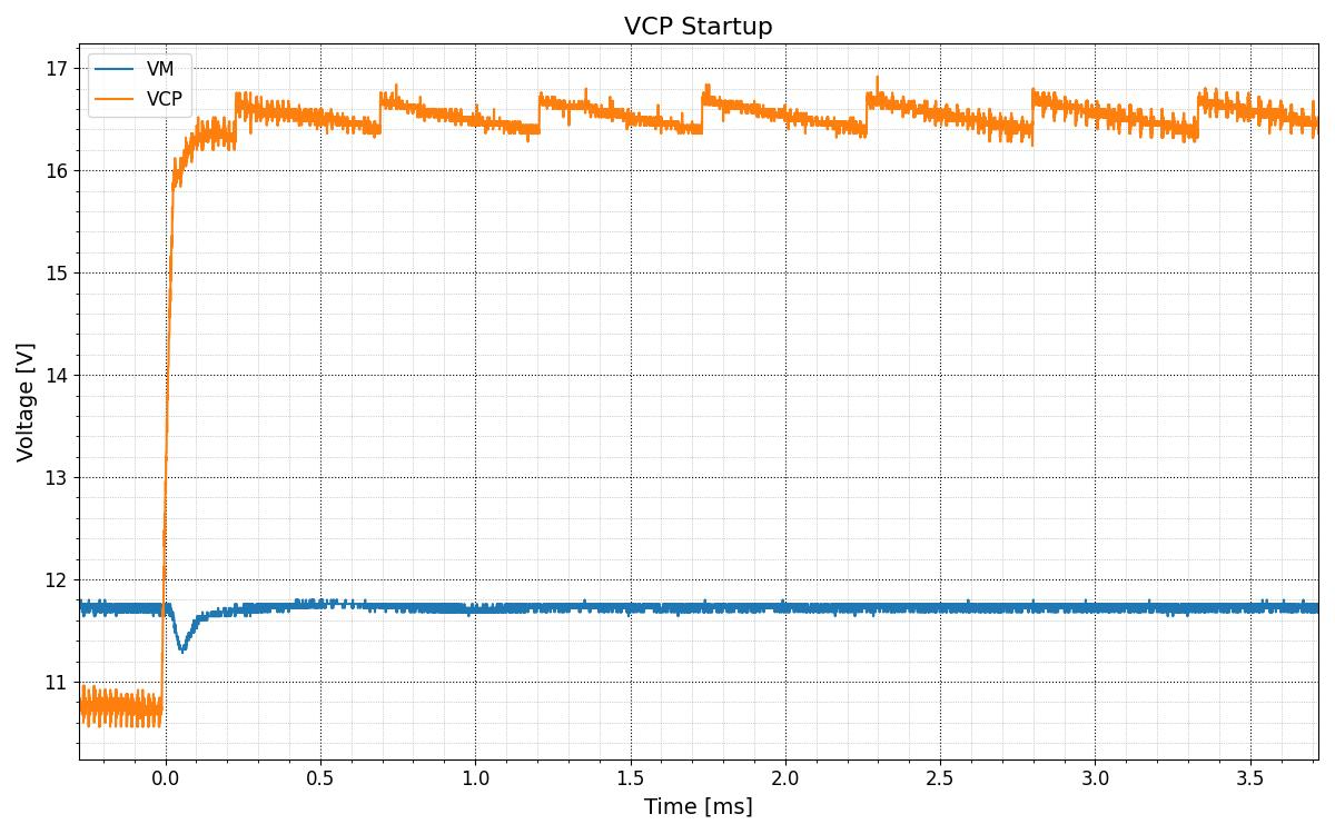
The plot shows an initial voltage drop of $200\, mV$ due to the charge pump current. The average charging current can be calculated by
$$I_{avg} = \frac{C_{cp} \cdot \Delta V_{cp}}{t_{start}} = \frac{220\,nF \cdot 5\,V}{200\,\mu s} = 5.5\,mA$$
From the VCP measurement the pulse skipping of the charge pump can be observed. When the VCP voltage drop below the threshold the charge pump uses burst mode operation to quickly recharge the capacitor. This creates the characteristic sawtooth waveform.
RPP Measurememt
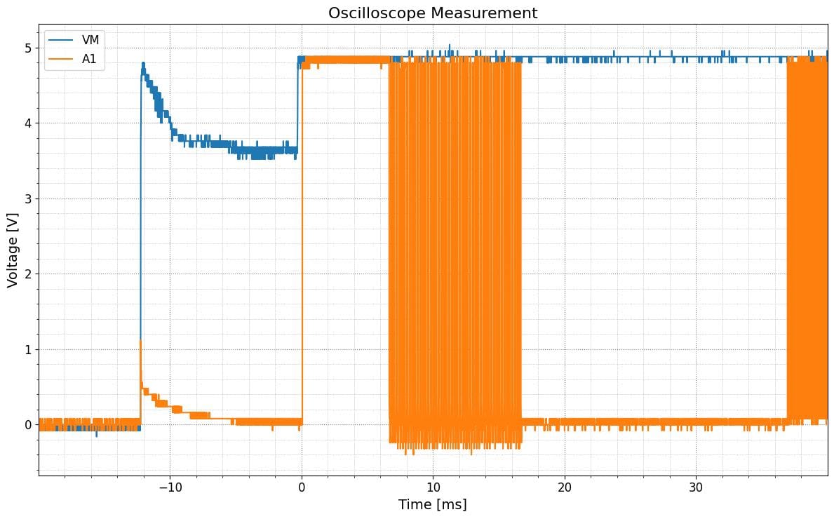
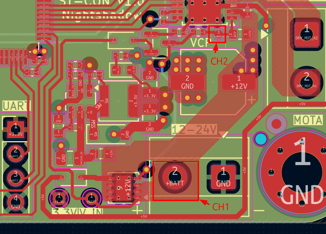
To check if the RPP is properly powered up with the GDU and the VCP, I measured the voltage drop across the input N-Channel MOSFET. See the schematic and PCB images below for the measurement points.
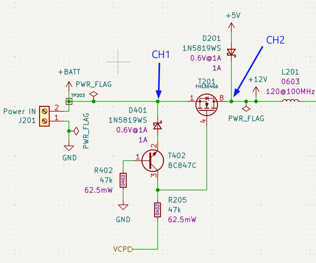
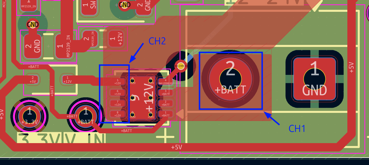
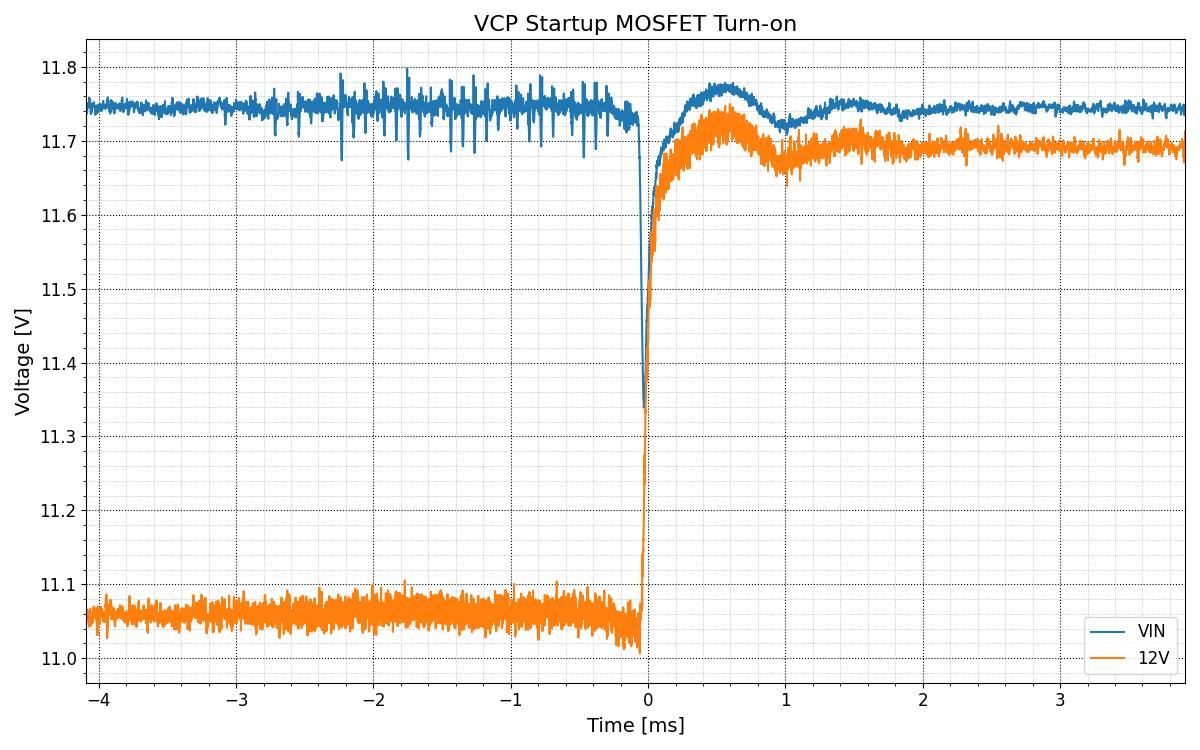
I set the trigger on the rising edge of the 12V. From the plot we can see that there is a voltage difference before of around 0.65\,V after enabling the GDU and the VCP turns on the RPP MOSFET the voltage drop is reduced to roughly $50\,mV$. This show that the RPP is fully turned on and the circuit is working as expected. For safety application were the functionality of the RPP must be guaranted this kind of measurement would allow to diagnose the MOSFET at the startup. This could be achieve by either the measurement of the 12V net (after the MOSFET) beofore and after enabling the GDU and calcualting the difference. In this case a steady supply voltage must be assumed else the measurement can not be garantued. A safer measurement requires to measure both nets VM and VIN as I did.
Side Quest Stepper Controll for MPS
One Stepper board with the original placed component (DRV8424) was used to drive a stepper motor for the calibration/correction of the Motor Position Sensor (MPS) V1.0
Revision 2.0 Updates
- Header Clearance: The NRF module footprint is located too close to the TC2050 debug header, causing mechanical interference.
- Transmitter Migration: Plan to upgrade from the NRF24L01 module to an ExpressLRS (ELRS) based transceiver operating at 2.4GHz for improved link reliability and telemetry. Mainly relevant for another project for this board which is a DIY Balancing Robot V1.0 . More on that in one of the next blog post though :)
Related Projects
- Motor Position Sensor (MPS) V1.0
- DIY Balancing Robot V1.0 (TBD)
Links
Datasheets
- https://www.ti.com/lit/ds/symlink/drv8424e.pdf?ts=1787419993512
- https://www.ti.com/lit/ds/symlink/drv8424.pdf?ts=1787382252197&ref_url=https%253A%252F%252Fwww.ti.com%252Fproduct%252Fde-de%252FDRV8424
- https://www.ti.com/lit/gpn/drv8702-q1